

In the past three years, the United States has carried out the largest – scale industrial restructuring in history around semiconductors. From the subsidies under the “CHIPS Act”, to the competition among states to introduce wafer fabs, and then to the expansion of R & D centers by industry giants, the semiconductor landscape in the United States is changing at an accelerated pace. The following map of the U.S. semiconductor ecosystem drawn by SIA shows the breadth of the industry with a dense array of dots. It includes locations for research and development (R & D), providers of intellectual property and chip design software, chip design, semiconductor manufacturing (wafer foundry), and manufacturing sites for semiconductor manufacturing equipment and material suppliers.
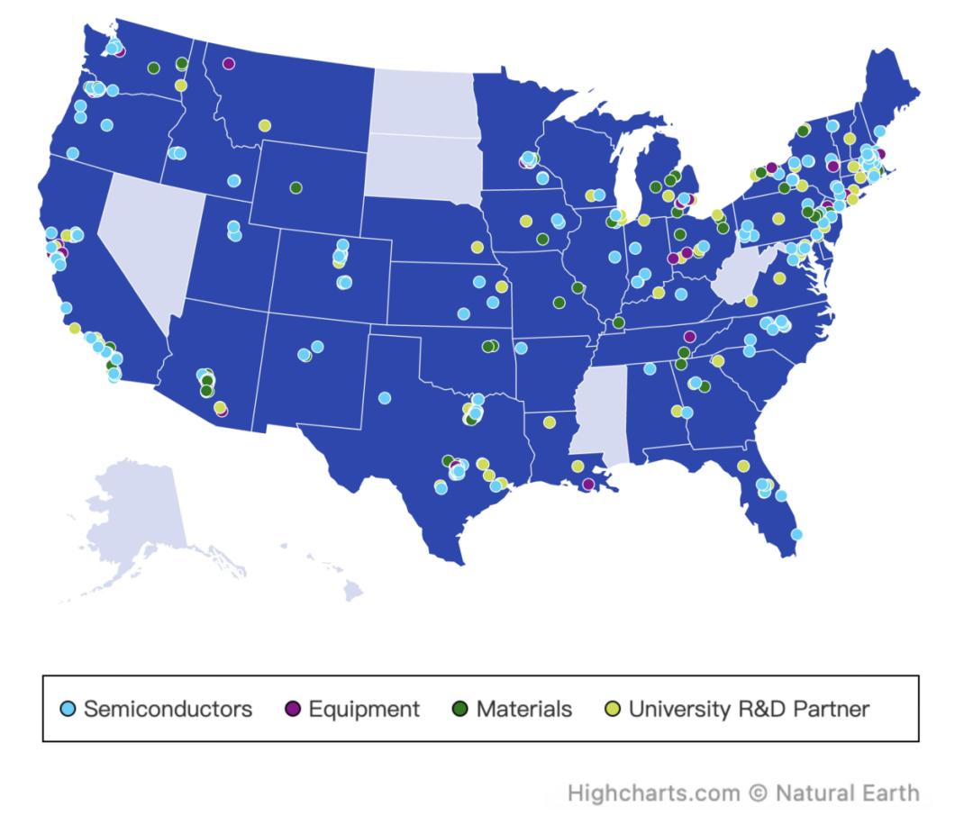
Next, we will systematically sort out the spatial layout and functional division of labor of the U.S. semiconductor industry by state and region.
(1) California: The world’s largest integrated cluster of “design – software – IP – equipment”
Most of the U.S. fabless companies are concentrated in California (CA), centered around the axis of San Jose – Santa Clara – San Diego, and extending to Irvine, Los Angeles, and Seattle. Together, they form a “computing innovation corridor” covering GPUs, AI, mobile communications, and server SoCs.
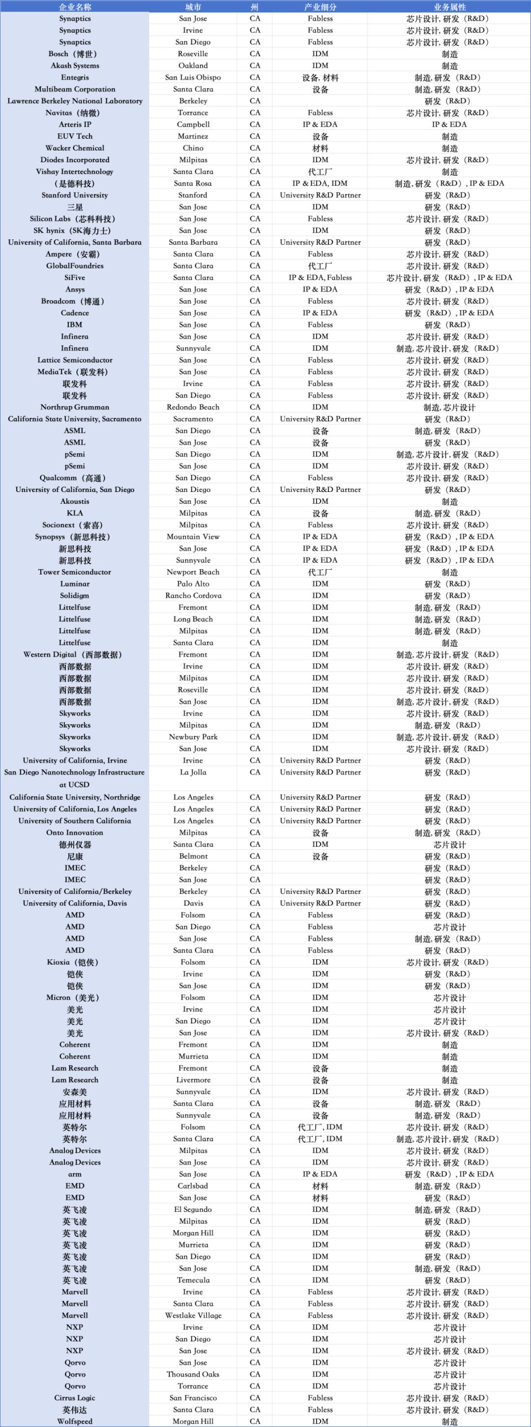
Semiconductor ecological layout in California
In this area, almost all the most influential chip design companies are clustered here, including NVIDIA, AMD, Broadcom, Qualcomm, Marvell, MediaTek, Silicon Labs, Synaptics, Cirrus Logic, Socionext, Navitas, Ampere, SiFive, Lattice Semiconductor and a series of other enterprises. These fabless companies are the “source of vitality” for the U.S. chip innovation system.
In addition to fabless companies, California is also the global core hub for EDA and IP. Synopsys has a presence in multiple cities in Silicon Valley, Cadence is located in San Jose and Boston, and both Arm and Ansys are in San Jose, forming the absolute center of the global chip design toolchain and IP ecosystem.
Meanwhile, California also has systematic advantages in the field of semiconductor equipment and materials. The U.S. headquarters of ASML is located in Silicon Valley. Lam Research is distributed in Fremont and Livermore. Applied Materials is located in Santa Clara and Sunnyvale. KLA has a manufacturing and R & D center in Milpitas, and together with material suppliers such as Entegris, Coherent, and Wacker Chemical, they form the most complete advanced manufacturing equipment ecosystem in the United States.
Generally speaking, California remains the “brain” of the U.S. semiconductor industry, controlling the four core points of algorithms, design, EDA, equipment, and IP, and firmly locking in the high – end of the global value chain.
(2) Arizona: The new U.S. wafer manufacturing center (powered by TSMC + Intel)
In the past 20 years, the focus of U.S. wafer manufacturing has gradually shifted south from California and Oregon to Arizona (AZ). The main reasons are: supply – chain security (away from earthquake zones), more lenient environmental and construction policies, significantly better basic conditions such as land and electricity, and the “CHIPS Act” funds being mainly directed towards Arizona.
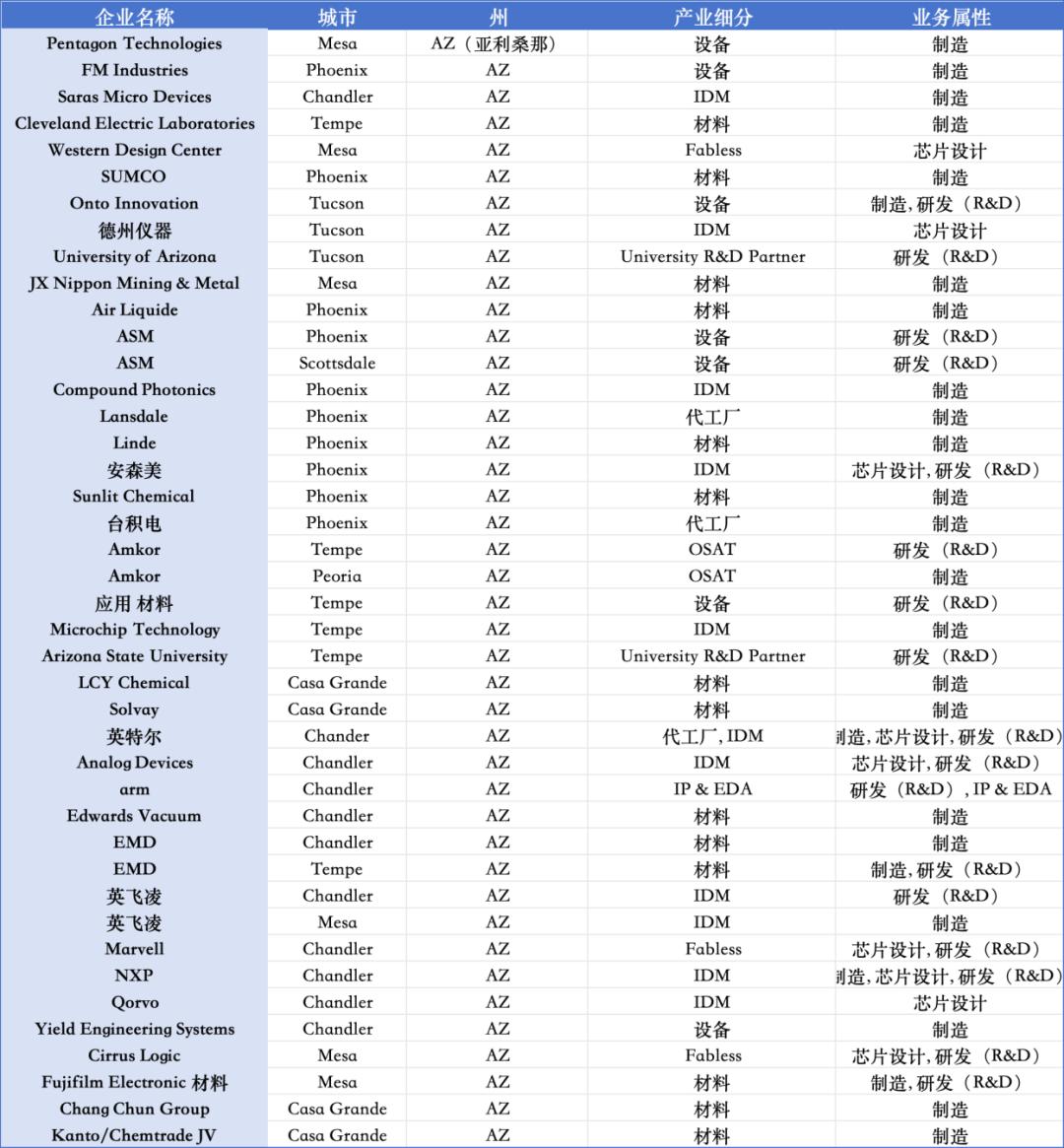
Semiconductor ecological layout in Arizona
In Arizona, TSMC’s Phoenix factory is the core base for advanced processes. Intel’s Chandler factory is one of the most critical advanced – process R & D centers in the United States. Amkor’s factory in Peoria is the largest OSAT base in the United States. In addition, IDM and fabless companies such as NXP, onsemi, Analog Devices, Infineon, Marvell, Qorvo, and Cirrus Logic have comprehensive layouts here.
More notably, Arizona has the most complete semiconductor material supply system in the United States, including key material suppliers such as SUMCO, Air Liquide, LCY Chemical, Sunlit Chemical, JX Nippon, and Solvay. The equipment capabilities are covered by ASM, Applied Materials, Onto Innovation, Yield Engineering Systems, etc., forming a complete manufacturing equipment ecosystem. The scientific research strength is provided by Arizona State University and the University of Arizona, which offer continuous talent and technological support.
In the United States, Arizona is the only region that has a complete semiconductor ecosystem with advanced processes (TSMC + Intel), OSAT (Amkor), a material system, an equipment system, IDM, fabless companies, and a university cluster. The United States is building a “second Hsinchu Science Park in Taiwan, China” in Arizona, reconstructing the complete capabilities from advanced processes to system packaging locally and avoiding geopolitical risks in the global manufacturing chain, making Arizona the main axis for U.S. wafer manufacturing in the next 10 – 20 years.
(3) Texas: The largest U.S. center for IDM, MCU, and automotive electronics
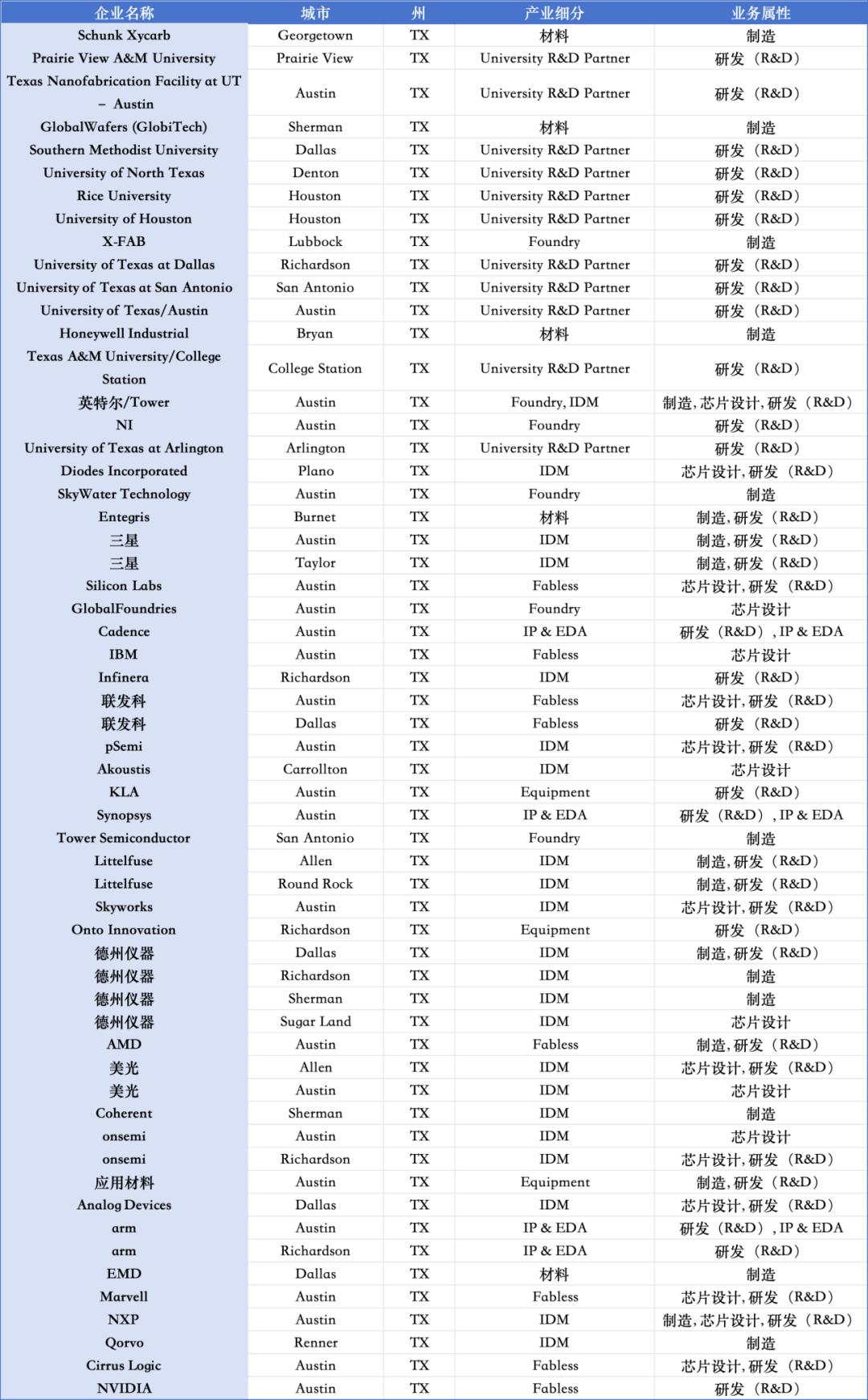
Semiconductor ecological layout in Texas
As can be seen from the map, Marvell, MediaTek, Cirrus Logic, AMD, IBM, Silicon Labs, and NVIDIA have all established important design centers in Texas, including in Austin, Dallas, and Allen. Different from California, Texas is not a traditional origin of fabless companies, but it has long – standing two key advantages:
A complete and large – scale system for automotive – grade and power chips (especially in the directions of electric vehicles and smart energy)
Strong demand for embedded applications (with a dense industrial foundation in industries such as industry, energy, oil, electricity, and manufacturing)
The core players include Texas Instruments (with operations in Dallas, Sherman, and Richardson), Samsung (in Austin and Taylor), NXP (in Austin), GlobalWafers (in Sherman), and Applied Materials (in Austin).
Due to this structure of “demand – driven + manufacturing roots”, Austin has gradually evolved into the second – most important innovation hub in the United States for AI SoC, MCU, DSP, and automotive – grade semiconductors, and has given rise to a different technological growth curve from California in the fields of automotive, power, and energy infrastructure.
Notably, with the transfer of Tesla, heavy – duty trucks, and power electronics to Texas, a new trend is emerging here: the automotive – grade power – embedded – AI control – MCU is forming a highly – coupled innovation chain, making Texas an irreplaceable new growth pole in the U.S. semiconductor landscape.
(4) The Northeast: The top – tier scientific research corridor for scientific research and R & D
The “Northeast Technology Corridor” stretching from New York (New York State) to Massachusetts (MA) and New Jersey (NJ) is the semiconductor region with the highest scientific research density in the United States. It is home to MIT, Harvard University, Boston University, Northeastern University, Cornell University, RPI (Rensselaer Polytechnic Institute), SUNY (the State University of New York system), Columbia University, New York University, as well as IMEC USA (the North American experimental center) and NY CREATES (the joint R & D platform of IBM, Micron, Applied Materials, and TEL).
The enterprise cluster also covers the core technology chain. IBM has established key R & D centers in Albany and Yorktown Heights, focusing on pushing the innovation frontier of semiconductor technology. GlobalFoundries has built one of the largest wafer manufacturing bases in the United States in Malta, providing important manufacturing capacity support. In addition, in Boston and its surrounding areas, there are many design and specialized chip companies such as Analog Devices (ADI), Skyworks in Andover, and MACOM, Qorvo, Marvell, and MediaTek, which together form a powerful cluster in the fields of analog, radio – frequency, and connectivity chips. Finally, Micron has also established an advanced manufacturing base in New York State.
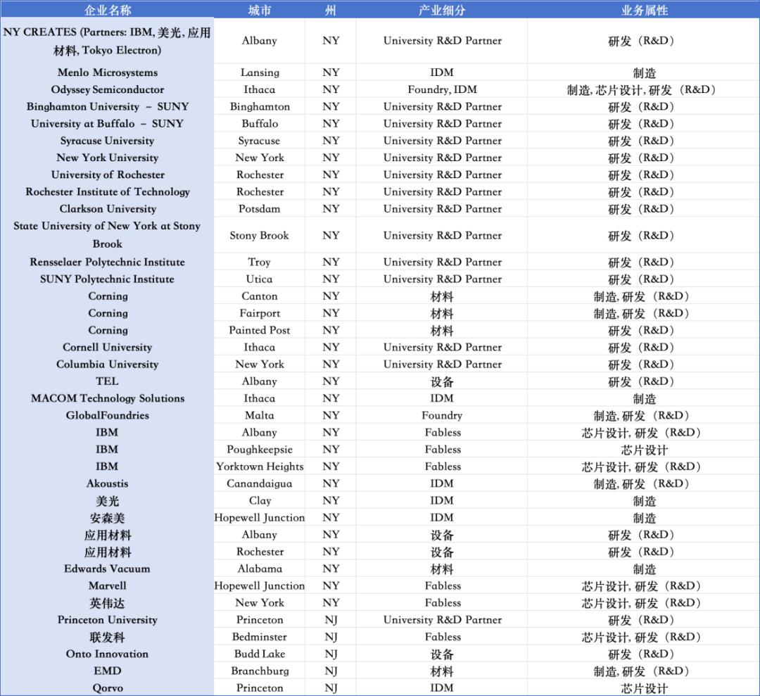
Semiconductor ecological layout in New York State and New Jersey
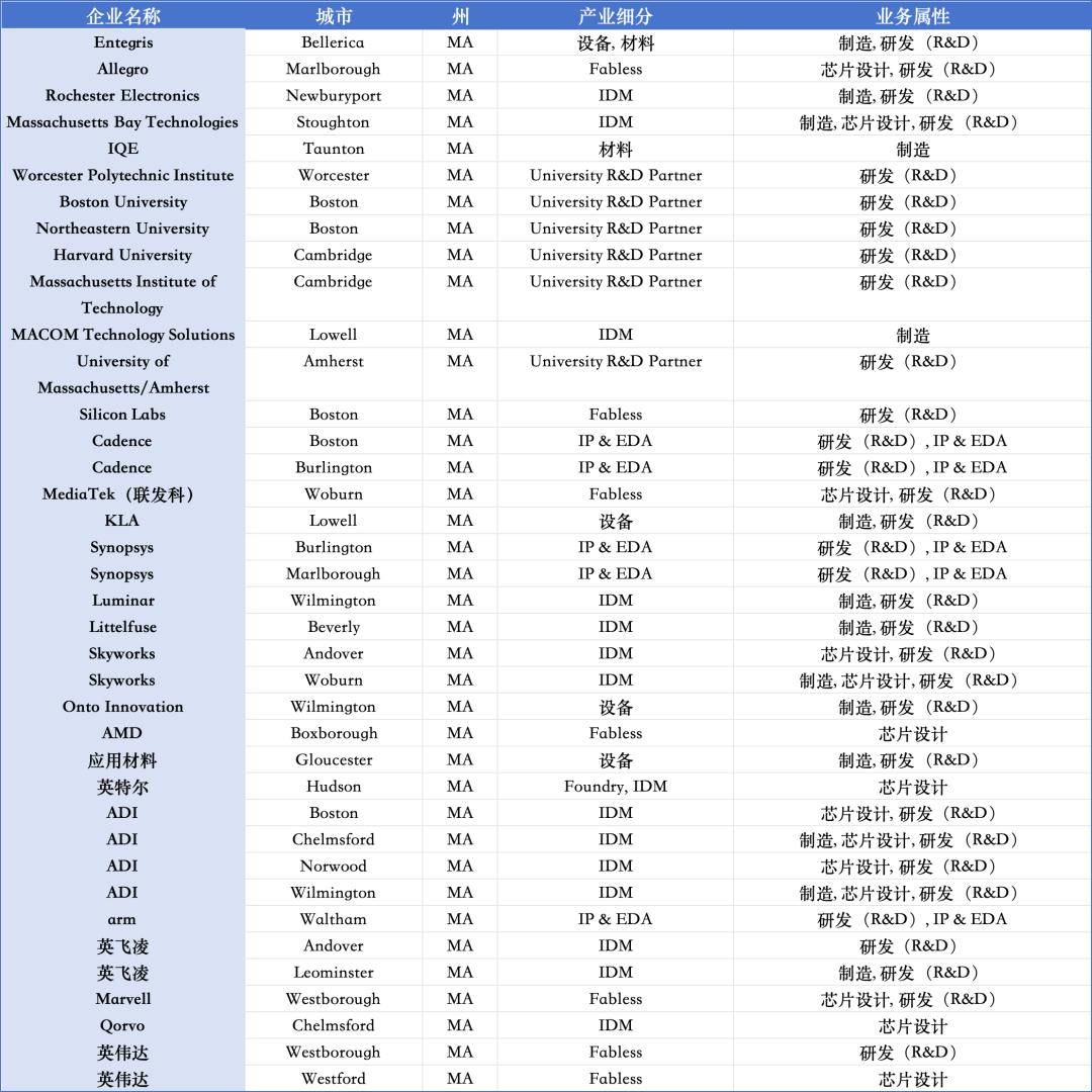
Semiconductor ecological layout in Massachusetts
This scientific research system actually extends north to Connecticut (CT) and Vermont (VT), and south to cover Delaware (DE), Washington, D.C. (DC), Maryland (MD), and Virginia (VA), forming a complete Northeast scientific research belt covering lithography equipment, materials science, defense electronics, and university research systems. For example, Connecticut has key lithography and material forces such as ASML and the University of Connecticut. Maryland aggregates R & D forces in military electronics and communications such as Northrup Grumman, Skyworks, and Johns Hopkins University. Delaware (DE) has a characteristic manufacturing system of DuPont Semiconductor Technologies, the University of Delaware, and Coherent. Vermont (VT) has a full – process manufacturing platform of GlobalFoundries Essex Junction.
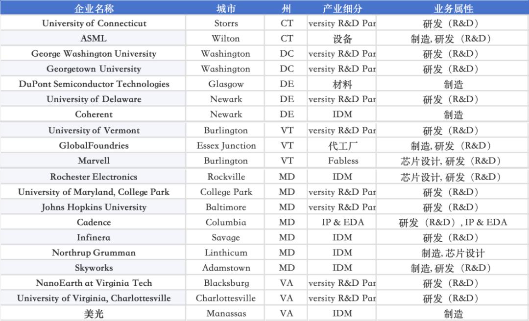
Semiconductor ecological layout in Connecticut (CT), Vermont (VT), Delaware (DE), Washington, D.C. (DC), Maryland (MD), and Virginia (VA)
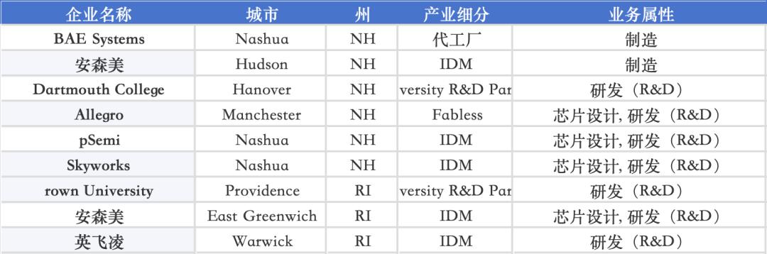
This scientific research belt also involves states in the New England region such as New Hampshire (NH) and Rhode Island (RI). In NH, there are clusters of defense electronics and radio – frequency IDM forces such as BAE Systems, onsemi, Allegro, pSemi, and Skyworks. In Rhode Island (RI), Brown University, onsemi, and Infineon form a collaborative system of “materials + power devices + university research”, further strengthening the in – depth connection of the Northeast region in defense electronics, power electronics, and research systems.
The “Northeast Scientific Research Corridor” can also extend south to Pennsylvania (PA), forming a complete “Mid – Atlantic Scientific Research System”. At the university research level, the University of Pennsylvania, Carnegie Mellon University, the University of Pittsburgh, Pennsylvania State University, and the Mid – Atlantic Nanotechnology Hub together form a full – link research system for materials, EDA, nanodevices, optical communications, and integrated systems. At the material end, enterprises such as EFC Gases & Advanced Materials, Wacker Chemical, EMD, and IQE form a supply chain for silicon wafers, high – purity materials, and epitaxial materials. In the manufacturing and IDM directions, Japanese Mitsubishi Semiconductor, as well as Coherent, Infinera, and onsemi, undertake characteristic manufacturing and optical communication device manufacturing capabilities. Ansys and Cadence constitute the R & D force for IP & EDA, and Broadcom also has a fabless business here, jointly promoting the deepening of the Northeast Corridor in the directions of “materials + EDA + IDM + optical communications + university research”.
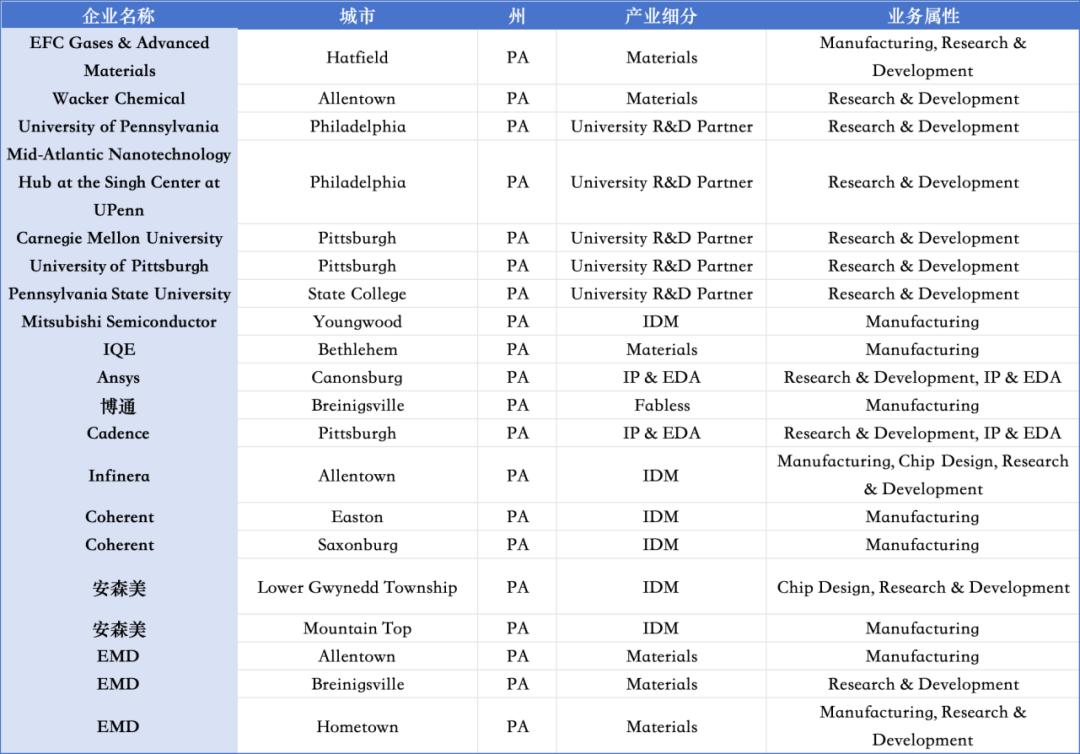
Semiconductor ecological layout in Pennsylvania
The Northeast Corridor is not a traditional manufacturing center, but it is the region in the entire U.S. semiconductor system with the deepest scientific research, the strongest materials, the most comprehensive metrology, and the most concentrated talent. It is the strategic origin for the United States to establish long – term technological advantages and a basic research system.
(5) The Northwest (Oregon – Washington – Colorado): The core manufacturing and material hub for Intel
The U.S. Northwest region consists of Oregon, Washington, and Colorado, with an industrial structure presenting a unique tripartite pattern of “process R & D + high – purity materials + high – end design”.
Hillsboro in Oregon is one of Intel’s most important process R & D centers in the world, on par with Chandler in Arizona. It is the core output location for Intel’s future node (EUV, High – NA, PowerVia, RibbonFET) roadmap. This region has formed a highly in – depth industrial cluster. The headquarters of Lattice Semiconductor is located here. Synopsys has an EDA R & D center here. Skyworks and Alpha & Omega Semiconductor are mainly engaged in IDM businesses for radio – frequency front – ends and power devices. Entegris, Siltronic, Mitsubishi Gas Chemicals, and Moses Lake Industries together form a key supply system for high – purity chemicals, silicon wafers, and process materials. Onto Innovation and Lam Research provide key front – end equipment such as detection, metrology, etching, and cleaning. Coupled with the layouts of onsemi, Microchip Technology, Qorvo, Allegro, Ampere, etc. in Beaverton, Eugene, Bend, Gresham, etc., the entire Oregon has formed a closed – loop from materials, equipment, wafer manufacturing to chip design.
In addition, universities and research institutions such as the University of Oregon, Oregon State University, and Portland State University continuously output talents and basic research in the directions of processes, materials, and devices.
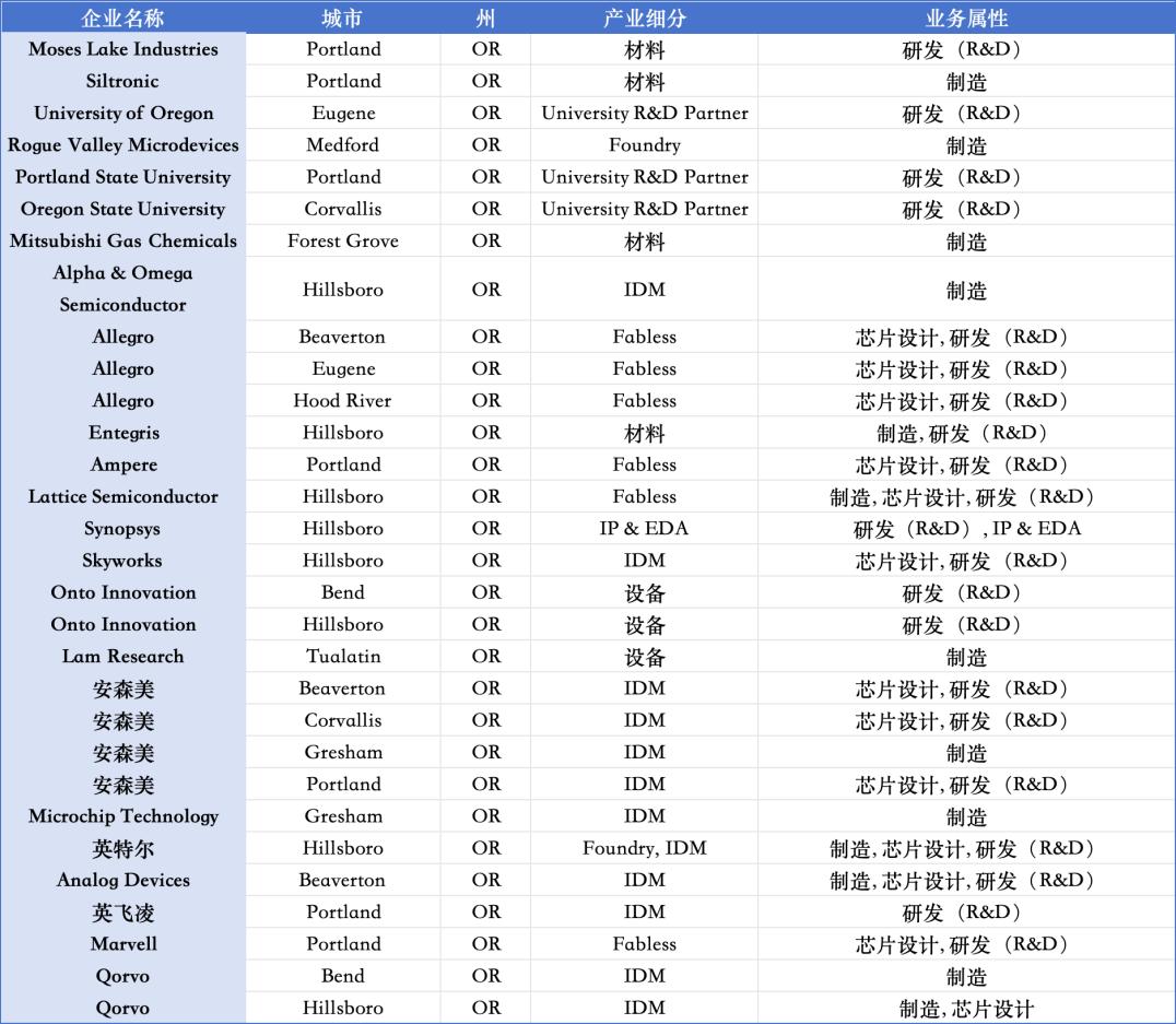
Semiconductor ecological layout in Oregon
The semiconductor industry in Washington State (WA)