
Device architecture and measurement setup
On a single chip, we fabricated an array of individual magnetic tunnel junction (MTJ) devices, each defined by a multilayered spintronic stack and embedded within a SiO2 dielectric matrix. The devices span a range of cross-sectional geometries, from circular to elliptical, with radii tailored to systematically probe thermal and structural scaling effects. As shown in Fig. 1a, d, the free layer (FL) comprises CoFe40B20(2)/Ta(0.21)/Ni80Fe20(7)/Ta(10)/ Ru(7), while a TiWN(15)/AlSiCu(100) sacrificial stack connects the active layers to the top contact. Magnetic stability is ensured by a synthetic antiferromagnet (SAF) structure consisting of Ta (5)/Ru (5)/IrMn (6)/CoFe30 (2)/Ru (0.7)/CoFe40B20 (2.6), and the bottom contact includes a thermally engineered Ta/CuN/Ru multilayer. All thicknesses are in nanometers. To enhance laser-induced heating, we employed a split feedline (FLine) and a transparent indium tin oxide (ITO) top contact52,53,54, enabling direct optical access to the active junction (Fig. 1a). The FL and SAF are separated by a crystalline MgO tunnel barrier, which facilitates spin-polarized tunneling by filtering electronic states based on wavefunction symmetry at the metal-oxide interfaces. Simultaneously, the MgO layer introduces thermal boundary resistance due to phonon-interface scattering. Its effective thermal conductivity is given by \(\kappa ={[{\kappa }_{{{\rm{B}}}}^{-1}+{({\kappa }_{{{\rm{I}}}}{t}_{{{\rm{MgO}}}})}^{-1}]}^{-1}\), where κB = 4.0 W m−1 K−1 is the intrinsic bulk thermal conductivity of MgO and κI = 2.5 × 10⁷ W m−2 K−1 represents the thermal conductance of the interface55. For an MgO thickness of 2 nm, this yields a remarkably low κ ≈ 0.05 W m−1 K−1, facilitating a steep temperature gradient (ΔT) across the barrier. This ΔT perturbs the thermal equilibrium between the ferromagnetic electrodes by broadening the carrier distribution in the heated layer relative to the cold one. The resulting energy-dependent imbalance in occupation probabilities, when filtered through the spin- and energy-selective transmission function \({\mathbb{T}}(E)\), gives rise to a net thermoelectric voltage. In the absence of electrical bias, this constitutes the tunnel magneto-Seebeck (TMS) effect, where the voltage arises solely from the thermally induced asymmetry. Under finite bias, the electrochemical potentials of the electrodes shift, altering the tunneling window and introducing additional asymmetry in the transport process. In this bias-enhanced regime (bTMS), the thermoelectric response reflects a nonlinear interplay between thermal excitation and electrically driven carrier flow. Both regimes are quantitatively described by the Landauer-Büttiker formalism, which links carrier occupation, spin-resolved density of states, and transmission asymmetry to the observed magneto-thermoelectric behavior46,50,56,57,58,59,60.
Fig. 1: Device, schematic measurement, and pure Seebeck signal.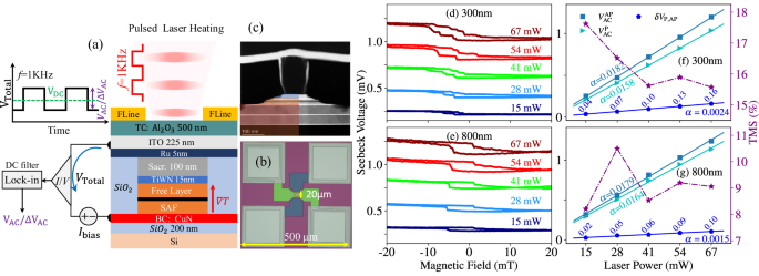
a Schematic of the device structure and complete measurement setup, including pulsed laser heating for thermal excitation, DC bias application, and lock-in detection of the thermoelectric voltage. b Optical microscope image of the fabricated device, showing the contact pads. c High-angle annular dark-field scanning transmission electron microscopy (HAADF-STEM) image of a magnetic tunnel junction (MTJ) nanopillar, highlighting the multilayer stack and structural integrity. d, e Thermoelectric voltage (VAC), measured via lock-in detection under open-circuit conditions (Ibias = 0), as a function of in-plane magnetic field for MTJs with nanopillar diameters of 300 nm (d) and 800 nm (e). Different curves correspond to varying laser powers (in mW). f, g Parallel-state voltage (\({V}_{{{\rm{AC}}}}^{P}\)), antiparallel-state voltage (\({V}_{{{\rm{AC}}}}^{AP}\)), the voltage contrast (δVP,AP), and the corresponding tunnel magneto-Seebeck (TMS) ratios as a function of laser power. Solid lines denote linear fits; slopes are reported as α.
Thermoelectric voltages were measured under zero bias (TMS) and finite bias (bTMS) conditions using a diode laser (λ = 638 nm) modulated at 1 kHz and focused on a ~7 μ spot using a calibrated knife edge method. The MTJ voltage was recorded simultaneously using a precision voltmeter, which yields the quasi-static component VDC, and by a lock-in amplifier referenced to the same 1 kHz modulation, isolating the dynamic thermoelectric response. The lock-in extracts the first harmonic—corresponding to the peak amplitude of the periodic thermovoltage—denoted VAC in the zero-bias (TMS) regime and ΔVAC when a DC bias is applied (bTMS). While a 50% duty cycle would in principle generate a DC thermovoltage under open-circuit conditions, our preamplifier’s AC-coupling blocks this offset, so that all analyses rely solely on the dynamic VAC signal. Under finite bias, the voltmeter concurrently measures a steady baseline voltage while the lock-in isolates the laser-synchronous modulation ΔVAC, thereby capturing the nonlinear interplay between thermal excitation and bias-driven tunneling.
Experimental results
Under open-circuit conditions (Ibias = 0), a laser-induced temperature gradient across the MgO barrier produces a spin-dependent thermovoltage VAC = S(B) ΔT, where S(B) is the field-dependent Seebeck coefficient reflecting the energy- and spin-resolved transmission asymmetry of the junction. As the in-plane field is swept, the magnetizations of the free layer and synthetic antiferromagnet switch between the parallel (P) and antiparallel (AP) states, tracing a hysteretic loop in VAC. In the saturated P and AP configurations, the thermovoltage plateaus obey \({V}_{{{\rm{AC}}}}^{{{\rm{P/AP}}}}={S}_{{{\rm{P/AP}}}}\Delta T\) thereby directly yielding the spin-dependent Seebeck coefficients SP and SAP. The magnitude of the tunnel magneto-Seebeck (TMS) effect is quantified as46,57,61,62:
$${{\rm{TMS}}}=\frac{{S}_{{{\rm{AP}}}}-{S}_{{{\rm{P}}}}}{\min (| {S}_{{{\rm{AP}}}}| ,| {S}_{{{\rm{P}}}}| )}\equiv \frac{{V}_{{{\rm{AC}}}}^{{{\rm{AP}}}}-{V}_{{{\rm{AC}}}}^{{{\rm{P}}}}}{\min \left(| {V}_{{{\rm{AC}}}}^{{{\rm{AP}}}}| ,| {V}_{{{\rm{AC}}}}^{{{\rm{P}}}}| \right)}.$$
(1)
To assess how the thermoelectric response scales with laser power, we measured VAC(B) at several optical power levels on devices with 300 nm and 800 nm nanopillar diameters, as shown in Fig. 1d, e, respectively. From each hysteresis loop, we extracted the plateau voltages \({V}_{{{\rm{AC}}}}^{{{\rm{P}}}}\), \({V}_{{{\rm{AC}}}}^{{{\rm{AP}}}}\), and computed their difference \(\delta {V}_{{{\rm{P,AP}}}}={V}_{{{\rm{AC}}}}^{{{\rm{AP}}}}-{V}_{{{\rm{AC}}}}^{{{\rm{P}}}}\). These quantities, together with the corresponding TMS ratio, are plotted versus laser power in Fig. 1f, g. In both devices, \({V}_{{{\rm{AC}}}}^{{{\rm{P}}}}\), \({V}_{{{\rm{AC}}}}^{{{\rm{AP}}}}\), and δVP,AP scale linearly with power (slopes α), consistent with the expected thermoelectric relation \({V}_{{{\rm{AC}}}}^{{{\rm{P/AP}}}}={S}_{{{\rm{P/AP}}}}\Delta T\). As the laser power increases to 67 mW, the resulting Seebeck voltages in our MTJ devices reach up to 1.5 mV—among the highest reported for thermally driven tunnel junctions—highlighting their potential for spin-caloritronic applications. Across all laser powers, the absolute Seebeck voltage is consistently 0.1 mV higher in 800 nm pillars compared to 300 nm ones. This likely reflects enhanced optical absorption and a larger number of spin-polarized carriers contributing to thermoelectric transport in the wider junction area. Meanwhile, the spin-dependent voltage contrast δVP,AP = (SP − SAP)ΔT is slightly higher in 300 nm devices—by approximately ~60 μV at 67 mW. A dedicated noise characterization, combined with COMSOL simulations to determine ΔT, would be required to assess the statistical significance and physical origin of trivial δVP,AP.
By applying a finite DC bias current Ibias, the junction operates in the bias-enhanced tunnel magneto-Seebeck (bTMS) regime. The bias changes the relative Fermi levels of the two electrodes, modifying the tunneling window and the weight of the thermally excited carriers that contribute to the signal61,63. Consequently, the measured thermovoltage becomes a nonlinear function of both Ibias and ΔT, and the perfect antisymmetry of the zero-bias Seebeck response (dictated by Onsager reciprocity) is broken. This nonlinear behavior originates from the energy-dependent transport described by the Landauer-Büttiker formalism, which integrates over the full energy spectrum of tunneling electrons64,65. In particular, one finds for each magnetic alignment (P or AP):
$$\Delta {V}_{AC}^{{{\rm{P}}}/{{\rm{AP}}}} = \, {V}_{{{\rm{on}}}}-{V}_{{{\rm{off}}}}\\ = \, {S}_{{{\rm{P}}}/{{\rm{AP}}}}\,\Delta T+\left({R}_{{{\rm{P}}}/{{\rm{AP}}}}-\Delta {R}_{{{\rm{P}}}/{{\rm{AP}}}}\right)I-{R}_{{{\rm{P}}}/{{\rm{AP}}}}I$$
where R is the resistance of the non-heated MTJ, and R – ΔR the thermally induced resistance change under laser excitation. The first term is the intrinsic Seebeck voltage, while the second is the Ohmic shift from the bias current flowing through the heated resistance. Because S, R, and Δ R differ between the P and AP states, these two contributions can be reinforced or canceling depending on the magnetic alignment. By tuning Ibias, one can suppress the net voltage in one state while preserving it in the other, generating true on / off switching and bTMS contrasts far beyond linear TMS. To quantify the switching contrast, and in analogy with the established definitions of TMR and TMS ratios, we define the bTMS ratio as
$${{\rm{bTMS}}}=\frac{\Delta {V}_{{{\rm{AC}}}}^{{{\rm{AP}}}}-\Delta {V}_{{{\rm{AC}}}}^{{{\rm{P}}}}}{\min \left(\left\vert \Delta {V}_{{{\rm{AC}}}}^{{{\rm{P}}}}\right\vert ,\,\left\vert \Delta {V}_{{{\rm{AC}}}}^{{{\rm{AP}}}}\right\vert \right)},$$
(2)
a normalized, dimensionless metric of spin-dependent voltage contrast. Figure 2 shows resistance and VAC versus magnetic field for 600 nm and 800 nm devices, highlighting the synchronized switching behavior. The TMR curves exhibit discrete step-like features known as Barkhausen jumps66,67,68,69,70, whose physical origin fundamentally differs with device size. In 300 nm nanopillars (see Supplementary Note 2), where dimensions lie below the threshold for vortex formation, these jumps are attributed to abrupt domain wall depinning and motion across local pinning sites71,72. In larger devices (600–800 nm), which exceed the critical lateral dimension for vortex stability, the free layer supports complex vortex states—flux-closure configurations that minimize magnetostatic energy73,74,75. In these structures, resistance steps correspond to sudden displacements of the vortex core between pinning sites76. Strikingly, VAC(B) exhibits sharp spikes coinciding with the resistance step-like jumps. These arise from abrupt spin reconfigurations that modify spin-dependent tunneling asymmetries, making ΔVAC(B) highly sensitive to dynamic magnetic events. The systematic dependence of the spike patterns on nanopillar diameter further supports their origin in magnetization dynamics and highlights the potential of bTMS as a noninvasive probe of domain wall motion, vortex states, and pinning landscapes. Future micromagnetic simulations77, theoretical modeling, and time-resolved measurements will be essential to fully elucidate the underlying mechanisms. Moreover, the spiking thermovoltage response offers promising opportunities for high-precision magnetic sensing, multilevel memory, and neuromorphic architectures.
Fig. 2: Thermovoltage spiking and double switching.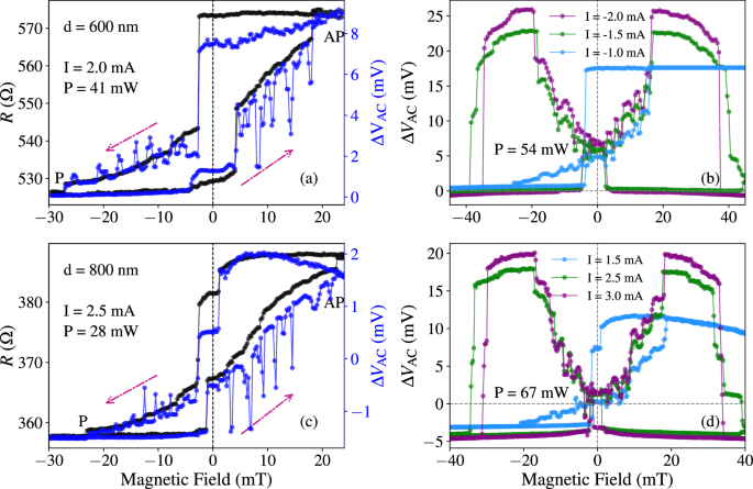
Measured ΔVAC and resistance as a function of magnetic field B for devices with diameters d = 600 nm (a) and d = 800 nm (c). Red arrows indicate the direction of the magnetic field sweep. Panels (b, d) show the threshold current and laser power required to induce double switching.
As shown in Fig. 2b, d, both resistance and thermovoltage traces reproducibly exhibit a double-switching behavior when the laser power and DC bias current exceed defined thresholds. This phenomenon—absent under purely thermal or electrical excitation—emerges consistently across all device sizes, indicating a robust physical basis. Crucially, rather than simply reflecting trivial coercivity reduction from heating, the combined thermal-electrical excitation drives the MTJ into a nonlinear, far-from-equilibrium regime where thermal gradients and electrical bias effects combine to create complex magnetization dynamics, resulting in multistable magnetization states and sequential switching thresholds. Additionally, high excitation levels may partially destabilize the nominally fixed SAF layer, subtly modifying interlayer coupling and enabling intermediate magnetization configurations. While all-optical switching78,79,80,81,82,83 employs ultrafast femtosecond laser pulses with extreme power densities to directly overcome magnetic energy barriers and switch fixed magnetic layers through rapid thermal demagnetization or helicity-dependent angular momentum transfer, our observed double-switching operates under continuous wave heating and electrical bias, representing a fundamentally different thermoelectric switching mechanism. This experimental observation establishes the foundation for targeted theoretical investigations to fully elucidate the underlying mechanisms and their implications for advanced spintronic technologies.
\(\Delta {V}_{{{\rm{AC}}}}^{{{\rm{P}}}}\) (Fig. 3a–c) and \(\Delta {V}_{{{\rm{AC}}}}^{{{\rm{AP}}}}\) (Fig. 3d–f) are plotted as functions of the bias current for various laser powers and nanopillar diameters. Both configurations exhibit distinctively nonlinear, cubic-like voltage responses to the applied bias current—features which we leverage explicitly in neuromorphic simulations, as detailed in the subsequent section. At a characteristic current (indicated by arrows in Fig. 3a–c), \(\Delta {V}_{{{\rm{AC}}}}^{{{\rm{P}}}}\) vanishes due to cancelation between Seebeck and bias-driven contributions—an effect absent in the AP state. This selective suppression significantly enhances the voltage contrast, resulting in sharp peaks in the bTMS ratio [Fig. 3g–i], and highlights the tunability of spin-caloritronic transport under combined thermal and electrical excitation. Although full conduction suppression is not achievable in MTJs, this configuration-dependent behavior mimics diode-like functionality and offers potential for selective spin-caloritronic readout.
Fig. 3: Bias-Enhanced Thermovoltage and bias-enhanced tunnel magneto-Seebeck (bTMS) Contrast in P and AP States.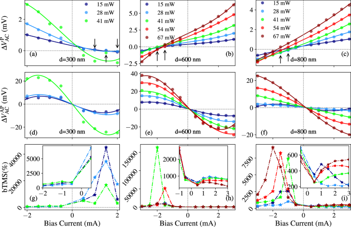
Measured ΔVAC as a function of bias current in P (a–c) and AP (d–f) states for devices with diameters of 300 nm, 600 nm, and 800 nm. Different curves correspond to varying laser powers (in mW). Solid lines correspond to cubic fits to the experimental data (V(I) = aI3 + bI2 + cI + d). Arrows in \(\Delta {V}_{{{\rm{AC}}}}^{{{\rm{P}}}}\) indicate points where the Seebeck and resistive contributions cancel out. g–i bTMS ratios with insets showing zoomed-in regions to clearly display the magnitude.
Proposal for efficient neuromorphic computing
The devices characterized in previous sections exhibit several properties that render them particularly advantageous for neuromorphic computing applications. These include operational versatility across multiple regimes—ranging from spike-based84, in-memory neuromorphic computing26, to direct exploitation of the inherent nonlinear processing capabilities observed in the bTMS regime. In this section, we focus on simulating the latter approach, and refer readers to Supplementary Notes 4 and 5 for discussions of alternative neuromorphic computing schemes. To exploit the nonlinear response of thermovolatges (Fig. 3) for neuromorphic computing, we propose the integrated circuit architecture illustrated in Fig. 4a. This platform combines spintronic MTJs with the precise optical control offered by vertical-cavity surface-emitting lasers (VCSELs), enabling spatially-resolved and programmable thermal excitation. Each VCSEL individually addresses an MTJ, inducing a localized thermal gradient and thereby activating the device’s spin-caloritronic response in a highly reconfigurable manner.
Fig. 4: Proposal of a spintronic chip for efficient neuromorphic computing.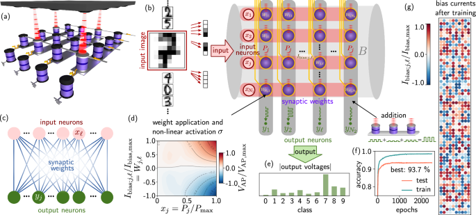
a Rending of the envisioned spintronic chip for neuromorphic computing. b Simulated operation of the neuromorphic chip in the bias-enhanced tunnel magneto-Seebeck (bTMS) regime for the task of handwritten digit recognition based on the 800 nm magnetic tunnel junctions characterised in Fig. 3f. The envisioned chip consists of 64 × 10 devices with one row corresponding to an entry in the input vector of dimension N1 = 64 and one column corresponding to an entry in the output vector of dimension N2 = 10 (one entry for each possible numeral). c This results in a densely connected single-layer neural network. The pixels of one input image are converted to a vector which serves as input encoded in the laser powers Pj (the laser powers are equal across one row). We apply a bias current Ibias;j,ℓ to each magnetic tunnel junction (MTJ) which serves the role of a trainable synaptic weight Wj,ℓ. d The nonlinear response of the MTJs to the laser power and bias currents enables neuromrophic computing with a high expressivity. The axes have been rescaled with \({I}_{{{\rm{bias}}},\max }=3.0{{\rm{mA}}}\), \({P}_{\max }=150{{\rm{mW}}}\), \({V}_{{{\rm{AP}}},\max }=23.35{{\rm{mV}}}\). The resulting Seebeck voltages are added across one column (dark grey) and (e) result in an output voltage. During training, the weights are adjusted so that the largest output voltage indicates the number shown in the image. Here, for an input image of 7, the network correctly predicts the output after training. f Training and test accuracy for the correct identification of images. g Bias currents (synaptic weights) across the chip after training. The higher the current, the more relevant a pixel for the correct classification.
To simulate the operation of such a neuromorphic chip, we consider the architecture illustrated in Fig. 4b and train the system to perform image classification on handwritten digits85 (Methods). Operating within the bTMS regime, we use the laser power Pj incident on a device in the jth row to encode the input (corresponding to one pixel in the image to be classified). We encode the synaptic weights Wj,ℓ in the bias currents applied to the device in the jth row and the ℓth column Ibias;j,ℓ. Leveraging the nonlinear dependence of the thermovoltaics on both current and laser power σ, Fig. 4d, each spintronic device applies a synaptic weight to the neuronal input values and computes a nonlinear activation function determined by the device characteristics. As a result, the MTJ in row j and column ℓ effectively computes the function:
$${\tilde{x}}_{j,\ell }=\frac{\Delta {V}_{{{\rm{AP}}};j,\ell }}{\Delta {V}_{{{\rm{AP}}},\max }}=\sigma \left(\frac{{P}_{j}}{{P}_{\max }},\frac{{I}_{{{\rm{bias}}};j,\ell }}{{I}_{{{\rm{bias}}},\max }}\right)=\sigma ({x}_{j},{W}_{j,\ell }),$$
(3)
with σ the nonlinear response of the device, ΔVAP;j,ℓ the AP voltage at the device in row j and column ℓ, \(\Delta {V}_{{{\rm{AP}}},\max }\) the maximum AP voltage recorded for a single device, \({I}_{{{\rm{bias}}},\max }\) the maximum current used in the experiment, and \({P}_{\max }\) the maximum laser power. The underlying crossbar array allows to add the resulting voltages and yields the neuronal output values. The total output voltage of one column in Fig. 4b then yields the output neuron:
$${y}_{\ell }= \sum_{j}{\tilde{x}}_{j,\ell }= \sum_{j}\sigma ({x}_{j},{W}_{j,\ell }).$$
(4)
This primary computational stage could be cascaded with additional processing elements, such as another MTJ (as depicted in Fig. 4a) or a memristor, to implement further nonlinear activation functions or incorporate additional neuronal layers (detailed in the Supplementary Notes 4 and 5). For the purpose of this simulation, we consider a single layer neural network mapping between input and output neurons (schematically represented in Fig. 4c), i.e., the resulting yℓ after a single layer is the output of our neuromorphic system. We use one-hot encoding, i.e., the entry yℓ corresponding to the largest output voltage determines the class—in this case the number shown in the image, Fig. 4e.
We plot the system’s accuracy on the training set and a test set of previously unseen images in Fig. 4f achieving a classification accuracy of 93.7 %. In Fig. 4g, we display the pattern of bias currents after training. Red circles indicate positions that are more relevant for the computation of the output, while white and blue circles denote less relevant parts. Note that red circles are mostly found in rows that correspond to pixels that contain the numerals.
Our neuromorphic platform—integrating optical inputs with MTJs—offers several advantages: (i) Optical injection via VCSELs eliminates the need for dedicated electrical wiring at each node, leading to a reduced spatial footprint and increased scalability for high-density chip integration86,87. While individual MTJs can be scaled down to widths of tens of nanometers88, the ≈ 5 × 5 μ m2 footprint of a single VCSEL emitter89 limits integration density. Our shared-addressing architecture—where each VCSEL optically addresses multiple MTJs—overcomes this constraint, enabling chips with millions of devices per square millimetre in an industrial setting. (ii) The pulsed operation of the laser allows for efficient batch processing since sequences of pulses can be used to encode different data inputs. This could become particularly interesting in the context of sequence modelling which is a fundamental capability of large language models. Furthermore, using frequency multiplexing on the laser light and demultiplexing on the output voltages, information can be encoded at different pulse frequencies allowing for spatially efficient parallel processing (see Supplementary Notes 4 and 5). (iii) Since the proposed device bridges between an optically encoded input and electronic output in a relatively high voltage range, the device could also become an important component of hybrid chips combining optical neural networks with analog electronics or complementary metal-oxide-semiconductor (CMOS)-based neuromorphic chips.