
Chemicals and materials
Natural Kish graphite crystals (Grade 300, 99.99% purity) were procured from Graphene Supermarket. Hexagonal boron nitride crystals were provided by T. Taniguchi and K. Watanabe, and were used as received. Large, flat crystals of RuCl3 were grown by chemical vapour transport following the procedure detailed in a previous study41. Briefly, commercial RuCl3 powder (Alfa Aesar, anhydrous, Ru ≥ 47.7%) was loaded into a quartz ampoule in an argon glovebox, sealed under dynamic vacuum, and heated in a two-zone furnace with a temperature gradient and ramp rates of 1 K per min. The resulting crystals were collected from the cold end and stored in an argon-filled glovebox.
Si/SiO2 wafers (0.5-mm-thick, 285 nm SiO2) and polydimethylsiloxane stamps (PDMS) were obtained from NOVA Electronic Materials and MTI Corporation, respectively. Sn/In alloy (Custom Thermoelectric), poly(bisphenol-A carbonate), hexaammineruthenium(III) chloride (98%) and potassium chloride (>99%) were purchased from Sigma-Aldrich. Sulfuric acid (ACS grade, >95−98%, Thermo Fisher Scientific) was used as received. All aqueous electrolyte solutions were prepared using type I water (EMD Millipore, 18.2 MΩ cm). Solid KCl was added as a supporting electrolyte in Ru(NH3)63+ solution to a final concentration of 100 mM.
Sample fabrication
Graphene and hBN flakes were mechanically exfoliated onto SiO2 (285 nm)/Si substrates from bulk crystals using Scotch tape42. Exfoliated flakes on SiO2/Si chips were identified by optical microscopy (Laxco LMC-5000). MLG flakes were distinguished by their approximately 7% optical contrast in the green channel14,43 and further verified by Raman spectroscopy (HORIBA LabRAM Evo). Extended Data Fig. 1 shows a representative optical contrast of around 7% in the green channel for MLG and about 14% for bilayer graphene. The thickness of hBN flakes was determined by atomic force microscopy (Park Systems NX10) (Extended Data Fig. 1c,d).
α-RuCl3 crystals were exfoliated in an argon-filled glovebox onto SiO2 (90 nm)/Si substrates to prevent degradation. Precise thickness control was not required, as even a single monolayer of α-RuCl3 is sufficient to induce substantial hole doping in graphene30,41. Instead, emphasis was placed on selecting flakes smaller than the hBN to ensure complete encapsulation, and flatness was prioritized to minimize strain during stacking. Suitable flakes were identified with an optical microscope (Nikon) within the glovebox.
We selected the multilayer system comprising graphene, hBN, RuCl3 and WSe2 due to their complementary characteristics. Graphene offers a tunable and well-defined electronic platform, whereas hBN serves as an inert spacer that allows precise control of doping. The RuCl3 and WSe2 layers function as stable charge-transfer dopants, modulating graphene’s electronic properties without affecting its structural integrity. Together, these materials enable systematic tuning of interfacial doping while preserving the overall structural quality of the heterostructure. MLG–hBN–RuCl3 heterostructures were assembled by a dry-transfer technique on a temperature controlled stage (Instec), equipped with an optical microscope (Mitutoyo FS70) and micromanipulator (MP-285, Sutter Instrument) in an argon glovebox. A poly(bisphenol-A carbonate) film on a PDMS stamp was used to pick up a RuCl3 flake within 30 min of exfoliation to minimize moisture exposure, which could compromise its doping efficacy41. The picked RuCl3 flake was then capped with an hBN flake (3–180 nm thick), followed by MLG, partially overlapping the RuCl3 to leave a segment of graphene without RuCl3. A thick graphite flake (10–100 nm) was finally transferred to partially overlap the graphene, providing electrical contact with the heterostructure. The poly(bisphenol-A carbonate) film was delaminated from the PDMS stamp and placed onto a clean SiO2/Si chip. Electrical contacts with graphite were subsequently established using Sn/In microsoldering14.
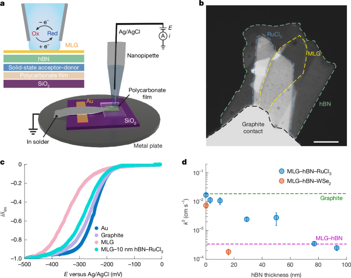
SECCM measurements
Single-channel SECCM nanopipettes were fabricated from quartz capillaries (0.7 mm inner diameter, 1 mm outer diameter; Sutter Instrument) using a laser puller (P-2000, Sutter Instrument) with the following parameters: heat = 700, filament = 4, velocity = 20, delay = 127, and pull = 140. This procedure yielded pipettes with orifice diameters of 600–800 nm, as confirmed by bright-field transmission electron microscopy (TEM; Extended Data Fig. 3). Each nanopipette was filled with an electrolyte solution containing the redox species of interest and equipped with a silver wire coated with AgCl, serving as a quasi-reference or counter electrode.
Scanning electrochemical cell microscopy experiments were performed using a Park NX10 SICM module. The nanopipette was positioned above the sample using an optical microscope and approached the surface at 100 nm s–1 until meniscus contact was detected by a current increase above 3 pA. During approach, a −0.5 V bias was applied to facilitate diffusion-limited reactions. Cyclic voltammograms were recorded at multiple locations by sweeping the potential at 100 mV s−1 between –0.6 V and 0 V, with the half-wave potential, E1/2, defined as the potential at which i = i∞/2, where i∞ represents the diffusion-limited current plateau. [Ru(NH3)63+/2+] was chosen as the redox couple because it has well-characterized, reversible, outer-sphere ET with no detectable adsorption on graphite electrodes, as confirmed by in situ Raman spectroscopy14,21. This ensures that the measured kinetics are sensitive to the electronic properties of the electrode while avoiding complications from surface-specific reactions.
Measurements were conducted on multiple independently fabricated devices, each featuring a distinct hBN thickness and comprising regions of evaporated gold as well as MLG with and without RuCl3. Notably, the thickness data for 0- and 3-nm-thick hBN were measured on the same device, as were the data for 77- and 93-nm-thick hBN. For devices without hBN, RuCl3 and WSe2 are sensitive to air exposure, so the entire MLG was used to encapsulate them and, consequently, no isolated MLG regions were available.
For each device, we recorded 1–2 voltammetric cycles at multiple spatially separated positions to ensure reproducibility and capture local variability. Voltammetric data from each MLG position, including multiple cycles, were binned and individually fitted to COMSOL simulations to extract k0 values. The gold regions served as an internal reference, with their data fitted using a reversible rate constant of 0.5 cm s–1 to account for any variations E0. This yielded multiple k0 values per device. The values plotted in Fig. 1d represent averages across these measurements, with error bars indicating the standard deviation. All extracted k0 values are provided in Extended Data Table 1. We find that the enhancements in k0 observed here far exceed those predicted by MHC theory, consistent with other studies that have reported similar limitations of the MHC framework18,19,20,44,45,46.
Although our devices were measured on the same day as fabrication, a 4–5 h interval was required for device assembly—including stacking, making electrical contacts, and transfer to the SECCM measurement substrate—which may have contributed to the slower observed rates than reported in literature. In this context, having MLG regions without RuCl3–WSe2 on the same device provides a robust baseline to reliably study the relative enhancement in ET kinetics induced by these dopants.
Past contact angle studies on graphene report modest changes (from 105° to 90°) over several minutes47, which is significantly longer than our measurement timescale (<10 s). Molecular dynamics simulations show that increasing surface charge reduces wettability48, suggesting that electrowetting effects should be even weaker in doped graphene. Electrowetting experiments on highly oriented pyrolytic graphite in 0.1 M KF over a potential window of 0 to –2.0 V versus Ag/AgCl revealed negligible effects49, consistent with our experimental conditions (0.1 M KCl, 0 to –0.7 V versus Ag/AgCl). Our cyclic voltammetry signals remained stable, and microscopy before and after testing confirmed no detectable morphological changes. These observations indicate that electrowetting does not significantly affect our measurements.
Finite-element simulations
Finite-element simulations of steady-state cyclic voltammograms were performed using COMSOL Multiphysics (v.5.6)50, following a similar approach outlined in previous works14,21. The nanopipette geometry was modelled in a 2D axisymmetric configuration (Extended Data Fig. 2), with droplet radii assumed equal to the pipette aperture, consistent with past studies14,21,51. The pipette radius, as, and taper angle, θs, were determined from TEM images (Extended Data Fig. 3). A survey of multiple nanopipettes prepared under identical conditions revealed that the taper angles are highly consistent (14.1 ± 0. 3°), whereas the aperture sizes have a modest distribution ranging from 600 to 800 nm.
Mass transport of redox species was modelled using the ‘Transport of diluted species’ and ‘Electrostatics’ modules, solving the steady-state Nernst–Planck equation:
$$\begin{array}{c}{D}_{i}\,\left(\frac{{\partial }^{2}{c}_{i}}{\partial {r}^{2}}+\frac{1}{r}\frac{\partial {c}_{i}}{\partial r}+\frac{{\partial }^{2}{c}_{i}}{\partial {z}^{2}}\right)\\ \,=-\frac{{z}_{i}F{c}_{i}{D}_{i}}{RT}\left(\frac{{\partial }^{2}\phi }{\partial {r}^{2}}+\frac{1}{r}\frac{\partial \phi }{\partial r}+\frac{{\partial }^{2}\phi }{\partial {z}^{2}}\right);\,0 < r < {r}_{{\rm{s}}},0 < z < l\end{array}$$
(1)
where r and z represent the coordinates parallel and normal to the sample surface, respectively; F is the Faraday constant; and rs and l denote the width and height of the simulation space, respectively. The height l = 30 m was set to exceed the nanopipette aperture, ensuring boundary effects were negligible. The meniscus was modelled as a cylindrical droplet (height, h), consistent with the hydrophobic interaction of water on graphite (contact angle 90°)14,21. The electroactive radius, a, is set equal to the nanopipette radius as, in agreement with previous studies14,21. The variables ci, zi and Di represent the concentration, charge number and diffusion coefficient, respectively, of either the oxidized (cO) or the reduced (cR) form. The electric potential ϕ in solution is determined by solving the Poisson equation:
$$\frac{{\partial }^{2}\phi }{\partial {r}^{2}}+\frac{1}{r}\frac{\partial \phi }{\partial r}+\frac{{\partial }^{2}\phi }{\partial {z}^{2}}=-\frac{{\sum }_{i}{z}_{i}F{c}_{i}}{\varepsilon {\varepsilon }_{0}};\quad 0 < r < {r}_{{\rm{s}}},\,0 < z < l$$
(2)
where ε = 80 is the dielectric constant of the solvent (water), and ε0 is the vacuum permittivity. The terms ci and zi in equation (2) include the ions of the supporting electrolyte (0.1 M KCl) in addition to the redox-active species cO and cR. The rate of the heterogeneous electron-transfer reaction is governed by the Butler–Volmer equations:
$${k}_{{\rm{red}}}={k}^{0}{e}^{-\alpha \frac{F}{RT}({V}_{{\rm{app}}}-{E}_{0})}$$
(3)
$${k}_{{\rm{ox}}}={k}^{0}{e}^{(1-\alpha )\frac{F}{RT}({V}_{{\rm{app}}}-{E}_{0})}$$
(4)
where k0 is the standard rate constant, α is the transfer coefficient, E0 is the standard potential and Vapp is the applied electrochemical potential. For the simulation of \({\rm{Ru}}{({{\rm{NH}}}_{3})}_{6}^{3+/2+}\), only the oxidized form (cO) is initially present in the solution. The flux is considered zero except at the contact surface. The general boundary conditions are given as follows:
$${c}_{{\rm{O}}}={c}_{{\rm{O}}}^{* },\,{c}_{{\rm{R}}}={c}_{{\rm{R}}}^{* }=0;\quad 0 < r\le {r}_{{\rm{s}}},\,z=l\,(\text{bulk})$$
(5)
$$\begin{array}{c}\frac{\partial {c}_{i}}{\partial n}=0;\,0 < z\le h,\,r={a}_{s};\\ \,h < z < l,\,r=a+(z-h)\,\tan ({\theta }_{p})\,(\mathrm{no}\,\mathrm{flux})\end{array}$$
(6)
$${J}_{{\rm{O}}}=-{J}_{{\rm{R}}}={k}_{\mathrm{red}}{c}_{{\rm{O}}}-{k}_{\mathrm{ox}}{c}_{{\rm{R}}};\quad 0 < r\le {a}_{s},\,z=0\,(\mathrm{sample}\,\mathrm{surface}\,)$$
(7)
where JO and JR represent the inward flux of the oxidized and reduced forms, respectively, and \({c}_{{\rm{O}}}^{* }\) and \({c}_{{\rm{R}}}^{* }\) are the bulk concentrations. The \(\frac{\partial {c}_{i}}{\partial n}\) term is the normal derivative of the concentration. The potential drop across the Helmholtz layer is implemented by defining the surface charge density, σ, at the sample surface:
$$\sigma =\frac{({V}_{\mathrm{dl}}-\phi ){\varepsilon }_{{\rm{H}}}{\varepsilon }_{0}}{{d}_{{\rm{H}}}};\quad 0 < r\le {a}_{s},\,z=0$$
(8)
where εH = 6 and dH = 0.5 nm are the dielectric constant and thickness of the Helmholtz layer, respectively, yielding the double-layer capacitance Cdl = 10 μF cm–2; Vdl is the corresponding double-layer potential relative to the charge neutrality point. The steady-state current was calculated by integrating the total flux of the reactants (JO) normal to the sample surface:
$$i=2{\rm{\pi }}F{\int }_{0}^{{a}_{s}}{J}_{{\rm{O}}}r\,dr$$
(9)
The diffusion coefficients DO and DR for the Ru(NH3)63+/2+ couple were set to 8.43 × 10⁻⁶ cm2 s–1 and 1.19 × 10⁻⁵ cm2 s–1, respectively; α = 0.5 was used for all simulations, consistent with previous studies on graphene thin films14,21. Our observed rates for doped MLG are ≤0.02 cm s–1, and for graphite approximately 0.03 cm s–1, indicating that ET remains primarily kinetically controlled within the experimental window. E0 was determined from electrochemically reversible voltammograms obtained on gold electrodes immediately before the experiments on graphene.
To extract the standard rate constant k0 from experimental voltammograms, we performed finite-element simulations across a range of k0 values and computed residuals between simulated and experimental data via sigmoidal fitting. For each simulation, the coefficient of determination (R2) was calculated using least-squares minimization, with the optimal k0 corresponding to the maximum R2 (minimal residuals). This protocol is illustrated in Extended Data Fig. 4, where R2 values for simulated rates are plotted alongside representative voltammograms.
Quantum capacitance
Quantum capacitance (Cq) is a material-specific capacitance that arises from the DOS at the EF in low-dimensional materials such as graphene14,52. When an electric potential (Vapp) is applied across a solid–solution interface, an electric double layer (EDL) forms at the surface to screen the excess charge5,53. In low-dimensional systems such as MLG, this EDL functions not only as a charge screening layer but also as an electrostatic ‘gate’, shifting the Fermi level and dynamically altering the material’s carrier concentration through electron or hole doping. In the case of MLG, applying Vapp results in two potential contributions: Vq, which is the potential change due to Cq, and represents the shift in the chemical potential; and Vdl, the potential drop across the double layer itself. These two components are related by:
$${V}_{\mathrm{app}}={V}_{{\rm{q}}}+{V}_{\mathrm{dl}}$$
(10)
The EDL capacitance, Cdl, in an aqueous solution, is estimated around 10 μF cm−2, assuming a compact layer capacitance with little dependence on ionic strength54. The diffuse-layer capacitance is >100 μF cm−2 in 0.1 M KCl solution53 and can be neglected. The total capacitance Ctotal combines Cq and Cdl in series:
$$\frac{1}{{C}_{\mathrm{total}}}=\frac{1}{{C}_{{\rm{q}}}}+\frac{1}{{C}_{\mathrm{dl}}}$$
(11)
Calculating quantum capacitance for MLG
Quantum capacitance is fundamentally connected to the DOS at the Fermi level, which depends on the material’s band structure. For MLG, the quantum capacitance Cq can be expressed as:
$${C}_{{\rm{q}}}={e}^{2}\frac{dn}{d{V}_{{\rm{q}}}}$$
(12)
where e is the elementary charge, and \(\frac{dn}{d{V}_{{\rm{q}}}}\) represents the rate of change in carrier concentration n with respect to Vq. Under the two-dimensional free-electron gas model, considering graphene’s linear DOS near the Dirac point55, this relation simplifies to
$${C}_{{\rm{q}}}=\frac{2{e}^{2}{k}_{{\rm{B}}}T}{{\rm{\pi }}{\hbar }^{2}{v}_{{\rm{F}}}^{2}}ln\left[2\left(1+\cosh \left(\frac{e{V}_{\mathrm{ch}}}{{k}_{{\rm{B}}}T}\right)\right)\right],$$
(13)
where ħ is the reduced Planck constant, kB is the Boltzmann constant, vF ≈ c/300 is the Fermi velocity of Dirac electrons and Vch = EF/e is the graphene potential. At the Dirac point, where carrier concentration n is minimal, Cq approaches zero. At T = 300 K, the channel potential can be written as:
$$e{V}_{{\rm{ch}}}=\mu +e{V}_{{\rm{app}}}.$$
(14)
Assuming constant charge, the relationship between Cq and Cdl is
$$\frac{{C}_{{\rm{q}}}}{{C}_{\mathrm{dl}}}=\frac{{V}_{\mathrm{dl}}}{{V}_{{\rm{q}}}}.$$
(15)
Substituting Cdl = 0.1 F m–2 gives
$${V}_{\mathrm{dl}}=10\,{C}_{{\rm{q}}}{V}_{{\rm{q}}}.$$
(16)
This leads to the relation between Vq and the applied potential Vapp:
$${V}_{\mathrm{app}}=(1+10\,{C}_{{\rm{q}}}){V}_{{\rm{q}}}.$$
(17)
Finally, substituting equation (13) into equation (17) yields
$$\frac{{V}_{{\rm{q}}}}{{V}_{\mathrm{app}}}=1+10\times \frac{2{e}^{2}{k}_{{\rm{B}}}T}{{\rm{\pi }}{\hbar }^{2}{v}_{{\rm{F}}}^{2}}ln\left[2\left(1+\cosh \left(\frac{e{V}_{\mathrm{ch}}}{{k}_{{\rm{B}}}T}\right)\right)\right].$$
(18)
This expression provides Vq/Vapp as a function of Vapp, from which Vdl(Vapp) is extracted for different values of μ and incorporated into our COMSOL simulations to systematically account for quantum capacitance effects. Extended Data Fig. 5 shows the ratio Vq/Vapp as a function of applied potential at 300 K. The inset presents the corresponding Cq as a function of Vapp.
Raman spectroscopy measurementsSample preparation
The heterostructures used in this study were prepared using a dry transfer method in an argon-filled glovebox. A polymeric stamp consisting of poly(bisphenol-A carbonate) on PDMS was used to pick up a thin layer of hBN, thickness < 5 nm, which was then used to pick MLG and another hBN flake comprising steps of multiple thickness, ensuring that the multilayer hBN fully covered the MLG. The entire stamp was then placed onto freshly exfoliated RuCl3 on a Si/SiO2 substrate (90-nm-thick SiO2), and the PDMS was gently lifted at 160 °C, leaving behind the poly(bisphenol-A carbonate). The resulting structure consisted of Si/SiO2-RuCl3-multilayer hBN–MLG-thin hBN–PC. The thin hBN layer—large enough to cover the entire heterostructure—served as a capping layer to protect the stack from solvents. The poly(bisphenol-A carbonate) was then dissolved in chloroform for 15 min, leaving the heterostructure device ready for Raman measurements. Notably, doping is localized to the graphene in contact with α-RuCl3, forming an atomically sharp lateral junction30,41. During fabrication, defects such as gas bubbles trapped between layers or non-uniform strain distributions may modulate the coupling between the layers locally. This coupling controls charge transfer between graphene and α-RuCl3, as seen in the distance dependence introduced by hBN spacers. It is therefore crucial to freshly exfoliate RuCl3 just before stacking to avoid contamination, which could decouple the layers.
Spectra acquisition and analysis
Confocal Raman spectra were collected using a Horiba Multiline LabRam Evolution system with a 532 nm laser and 0.4–3 mW power, using either a 600- or 1,800-grooves-per-millimitre grating. Spectra were typically recorded with acquisition times of 5–10 s and 3–5 accumulations. The G peak position in the Raman spectra can be linearly correlated with the doping levels in graphene, particularly when modulated by the electric field effect30,41. In the MLG–RuCl3 device, the G peak is blue-shifted by more than 25 cm−1 relative to the region without RuCl3, indicating doping of approximately 2.5 × 10¹³ holes per cm2, consistent with previous studies30,41. Such studies have shown that the G and 2D peak shifts in graphene vary with doping induced by the electric field effect30,41, and the G peak shift has a quasi-linear dependence on doping. Averaging the slopes of the G peak shift versus carrier density across these studies yields a value of approximately 9 × 1011 cm−2 carriers per wavenumber shift in the G peak position. Voigt profiles are used to fit the peaks, accounting for the Lorentzian nature of the phonons and the Gaussian instrumental resolution30,41. A constant background is subtracted from each spectrum before fitting the peaks. The 2D peak position provides a sensitive probe of strain and morphological changes. Extended Data Fig. 6 shows negligible shifts in the 2D peak for MLG with and without hBN/RuCl3, across varying hBN thicknesses, thereby confirming the absence of significant geometric alteration.
First-principles modelling of doping in MLG/hBN/RuCl3 heterostructures
The MLG/hBN/RuCl3 heterostructure was modelled as a parallel-plate capacitor following Bokdam et al.32, with the Fermi level shift given by:
$$\Delta {E}_{{\rm{F}}}({E}_{{\rm{ext}}})=\pm \frac{\sqrt{1+2{D}_{0}\alpha {\left(\frac{d}{\kappa }\right)}^{2}| e({E}_{{\rm{ext}}}+{E}_{0})| }-1}{{D}_{0}\alpha d/\kappa }$$
(19)
Here, \(\alpha =\frac{{e}^{2}}{{\varepsilon }_{0}A}=34.93\) eV Å–1 (where A = 5.18 Å2 is the area of the graphene unit cell, and ε0 is vacuum permittivity), D0 = 0.102 eV−2 per unit cell (slope of MLG DOS), d is the dielectric spacer thickness, κ is relative permittivity and Eext is the external electric field. E0 accounts for any built-in electric field or doping potential.
Experimental validation of defect-mediated doping
To resolve the anomalous doping in thin hBN heterostructures (<20 nm), we fabricated devices with alternating hBN-supported (MLG/hBN/RuCl3) and suspended MLG regions using approximately 4-nm-thick hBN, as shown in Extended Data Fig. 7 (MLG/air/RuCl3). Doping levels were calculated using equation (19) and measured via Raman G-peak shifts (Extended Data Table 2).
The suspended region shows good agreement between theory and experiment. In contrast, the hBN-supported region has 21% higher doping than predicted. This discrepancy, along with the thickness-dependent deviations shown in Fig. 2e, suggests that defect states in hBN do contribute further charge transfer beyond classical capacitive coupling.
Liquid-activated fluorescence measurements
The sample was mounted on a Nikon Ti-E inverted fluorescence microscope equipped with a 100× oil-immersion objective lens (CFI Plan Apochromat λ 100×, NA = 1.45). Intensities in Fig. 3c were captured under 561 nm laser excitation (OBIS 561LS, Coherent, 165 mW) with an exposure time of 6 ms. Emission was collected after a band-pass filter (ET605/70m, Chroma).
Nanofabrication of Hall measurement devices
All device fabrication was performed in the Marvell Nanofabrication Laboratory. Electron beam lithography (CRESTEC CABL-UH system), with an A6 950 poly(methyl methacrylate) resist, was used to define the electrode and contact regions. Reactive ion etching (SEMI RIE system) exposed the graphene edges in the hBN–graphene–RuCl3 heterostructure through a sequence of plasma treatments: 15 s of O2 plasma to remove surface residues; 40 s of SF6/O2 plasma to etch through hBN and reveal the graphene; and a final 15 s of O2 plasma to eliminate etching by-products. Immediately following etching, Cr/Au (20/120 nm) was deposited by thermal evaporation (NRC Evaporator) at rates of 0.5 Å s–1 for Cr and 2–4 Å s–1 for Au to form electrical contacts and bonding pads. After lift-off, a second electron beam lithography step defined an etch mask for shaping the heterostructure into a Hall bar geometry, minimizing longitudinal and transverse resistance mixing. The poly(methyl methacrylate) mask was retained after fabrication to protect RuCl3 from environmental degradation. Device integrity was verified by measuring resistance between electrical contacts using a lock-in amplifier (Stanford Research SR830) on a probe station. Functional devices were wire bonded (TPT HB05) to 16-pin ceramic dual inline packages for subsequent measurements in a Quantum Design PPMS.
Theoretical preliminaries
The [Ru(NH3)6]2+/3+ redox couple is known to undergo ET through an outer-sphere mechanism, where the thermal fluctuations of long-ranged electrostatic interactions with the environment play a central role in mediating the dynamics56. In the weak-coupling (non-adiabatic) regime, the rate of interfacial reduction is well-described by the golden-rule expression6,57,
$${k}_{\mathrm{red}}({E}_{{\rm{F}}})=\frac{2{\rm{\pi }}}{\hbar }| V{| }^{2}{\int }_{-\infty }^{\infty }D(E){f}_{{E}_{{\rm{F}}}}(E){\langle \delta (\Delta E-E)\rangle }_{\mathrm{ox}}dE$$
(20)
$$=\,\frac{2{\rm{\pi }}}{\hbar }| V{| }^{2}{\int }_{-\infty }^{\infty }D(E){f}_{{E}_{{\rm{F}}}}(E){p}_{{E}_{{\rm{F}}}}^{{\rm{(ox)}}}(E)dE$$
(21)
Where V is the electronic coupling between the two redox states (assumed to be small); D(E) is the electrode’s DOS; \({f}_{{E}_{{\rm{F}}}}(E)\) is the Fermi–Dirac distribution, centred at the electrode’s Fermi level, EF;
$${f}_{{E}_{{\rm{F}}}}(E)=\frac{1}{1+{e}^{(E-{E}_{{\rm{F}}})/{k}_{{\rm{B}}}T}}$$
(22)
and \({p}_{{E}_{{\rm{F}}}}^{{\rm{(ox)}}}(\Delta E)\) is the equilibrium probability distribution of the vertical energy gap between the two charge transfer states, evaluated in the oxidized state. Under an assumption of linear dielectric response, the rate is appropriately computed with Marcus theory, where the energy gap obeys Gaussian statistics and the free energy surfaces of ET are parabolic6,7,
$$-{\rm{ln}}{p}_{{E}_{{\rm{F}}}}^{{\rm{(ox)}}}(E)=\frac{{(E-{E}_{{\rm{F}}}+\lambda )}^{2}}{4\lambda {k}_{{\rm{B}}}T}+\frac{1}{2}ln[4{\rm{\pi }}{k}_{{\rm{B}}}T]$$
(23)
An assumption of chemical equilibrium is made, such that the intersection of the Marcus curves is aligned with the electrode’s Fermi level58. The reorganization energy, λ—a critical determinant of the activation free energy—quantifies the reversible work required to deform the equilibrium solvation environment of a redox species into that of its counterpart without ET. Equivalently, λ represents the energy dissipated during a vertical transition, reflecting the solvent and electrode polarization response to instantaneous charge redistribution.
The effect of electrode metallicity on the reorganization energy
In outer sphere redox reactions, the electrostatic potential at the interface is critical in determining the ET rate59,60. As the Fermi level is shifted, the change in DOS renormalizes the material’s electrostatic interactions, reflecting variations in the material’s dielectric response function due to an altered number of charge carriers that can respond to external fields. Insight into this effect can be gained through simple models of electronic screening such as TF theory61,62 parametrized by a screening length, ℓTF, which sets the scale of exponential decay of electrostatic interactions in the material, and interpolates between a perfect metal (ℓTF = 0) and an insulating material (ℓTF → ∞). The screening length is closely related to a material’s low-energy electronic structure. In two dimensions, and for kBT < < EF, which is typically the case for the energy scale of valence electrons, ℓTF is63
$${{\ell }}_{\mathrm{TF}}=\frac{{{\epsilon }}^{(\mathrm{el})}}{2{\rm{\pi }}{e}^{2}D({E}_{{\rm{F}}})}$$
(24)
where n is the charge density of the material. Marcus derived dielectric continuum estimates of the reorganization energy for charge transfer with a perfect conductor ℓTF = 0 (ref. 7),
$$\lambda =-\frac{\delta {q}^{2}}{4{z}_{0}}\left(\frac{1}{{{\epsilon }}_{\infty }^{({\rm{sol}})}}-\frac{1}{{{\epsilon }}^{({\rm{sol}})}}\right)+{\lambda }_{{\rm{B}}},$$
(25)
where δq is the amount of transferred charge, \({{\epsilon }}_{\infty }^{({\rm{sol}})}\) and ϵ(sol) are the electrolyte’s optical and static dielectric constants respectively, z0 is the separation from the electrochemical interface, and λB is the bulk contribution to the reorganization energy, which dominates when far away from the interface. The \((1/{{\epsilon }}_{\infty }^{({\rm{sol}})}-1/{{\epsilon }}^{({\rm{sol}})})\) term, known as the Pekar factor64, is a measure of the free energy difference between a charge exclusively solvated by the medium’s fast (electronic) degrees of freedom, and that of a charge fully stabilized by the polarization field’s nuclear and electronic degrees of freedom.
The electrostatic potential at dielectric discontinuities can be obtained by solving Poisson’s equation with appropriate boundary conditions at the interface. If the two media that make up the interface are complex materials with some degree of unbound charge, the dielectric constant is replaced by a dielectric response function ϵ(r), and the non-local Poisson equation reads,
$$\nabla \cdot \int \,{d}^{3}{{\bf{r}}}^{{\prime} }{{\epsilon }}_{\alpha }({\bf{r}}-{{\bf{r}}}^{{\prime} })\nabla \phi ({{\bf{r}}}^{{\prime} })=-{\rho }_{\alpha }({\bf{r}})$$
(26)
where α labels the medium, and ρα(r) is the charge density in medium α. The boundary conditions to be satisfied are the continuity of the potential and the electric displacement field across the interface. For a point charge near a perfect conductor, the potential energy due to the conductor’s polarization in response to the external field can be mapped to the interaction between the real charge and an opposite-sign ‘image’ charge placed symmetrically inside the metal. The electrode contribution to the reorganization energy in equation (25) directly corresponds to the electrostatic interaction of a point charge δq with its image, weighted by the Pekar factor. It provides reasonable estimates of the reorganization energy at electrodes that approach the behaviour of an ideal conductor, but becomes inaccurate away from this limit. We have recently developed a formalism25—building on previous developments65,66,67—that describes how the solvent reorganization energy changes as a function of the electrode’s metallicity in the context of TF theory. If we consider the electrostatic boundary-value problem of a charge q embedded in a dielectric in contact with a material with finite TF screening, Poisson’s equation can be solved making use of Fourier-Bessel transforms65,66. The end result is an expression that encodes the interaction of the point charge q with the induced charge density in the electrode, as well as the self energy of the induced charge density. Although the Fourier–Bessel transform of the potential cannot be analytically inverted, an analogy can be made to the method of images to write the electrostatic potential energy of this system as the effective interaction of q with a modified image charge at −z0,
$$U({z}_{0},{{\ell }}_{\mathrm{TF}})=\frac{{q}^{2}{\xi }_{{{\ell }}_{\mathrm{TF}}}({z}_{0},{{\epsilon }}^{(\mathrm{sol})})}{4{{\epsilon }}^{(\mathrm{sol})}{z}_{0}}$$
(27)
where we have defined the image charge scaling function, \({\xi }_{{{\ell }}_{\mathrm{TF}}}({z}_{0},{{\epsilon }}^{(\mathrm{sol})})\), which informs on the value (with respect to q) of this fictitious image charge as a function of screening length ℓTF, and the dielectric constants of both media. It smoothly interpolates between the electrostatics at the boundary of an ideal conductor, and an insulator. We see that, at a fixed z0, the TF screening length in the electrode takes the image charge from −q to ξ∞(z0, ϵ(sol))q. The screening-dependent image potential results in a modified reorganization energy,
$$\lambda ({{\ell }}_{{\rm{TF}}})=\frac{\delta {q}^{2}}{4{z}_{0}}\left(\frac{{\xi }_{{{\ell }}_{{\rm{TF}}}}({z}_{0},{{\epsilon }}_{\infty }^{({\rm{sol}})})}{{{\epsilon }}_{\infty }^{({\rm{sol}})}}-\frac{{\xi }_{{{\ell }}_{{\rm{TF}}}}({z}_{0},{{\epsilon }}^{({\rm{sol}})})}{{{\epsilon }}^{({\rm{sol}})}}\right)+{\lambda }_{{\rm{B}}}$$
(28)
The term in parenthesis in equation (28) can be identified as a generalization of the Pekar factor, extended to describe the modulation of image interactions at the surface of a TF electrode.
Image interactions in hole-doped MLG
The low-energy band structure of graphene can be described analytically, obeying the well-known linear dispersion relation characteristic of massless Dirac fermions68. This in turn results in a linear electronic DOS,
$$D(E)=\frac{2}{{\rm{\pi }}{\hbar }^{2}{v}_{{\rm{F}}}^{2}}| E| $$
(29)
where vF ≈ 106 ms−1 is the Fermi velocity, and the electronic energy E is measured from the Dirac point. Under a low-temperature approximation, graphene’s charge density is69,
$$\rho ({E}_{{\rm{F}}})={\rm{sgn}}({E}_{{\rm{F}}})\frac{{{E}_{{\rm{F}}}}^{2}}{{\rm{\pi }}{\hbar }^{2}{v}_{{\rm{F}}}^{2}}$$
(30)
leading to an explicit relationship between ℓTF and the Fermi level70,
$${{\ell }}_{{\rm{TF}}}({E}_{{\rm{F}}})=\frac{{{\epsilon }}^{({\rm{el}})}{\hbar }^{2}{v}_{{\rm{F}}}^{2}}{4{e}^{2}| {E}_{{\rm{F}}}| }.$$
(31)
The separation of the redox ion from the electrode, z0, must be chosen judiciously. Given the outer-sphere nature of the reaction, it must account for the structure of the interface, including an adlayer of water molecules on the surface of the electrode that are tightly bound and held together by a hydrogen-bonding network71,72, as well as the inner coordination environment and the outer solvation shell of the redox species. On the other hand, as the diabatic coupling term typically decays exponentially with separation \(V\approx {V}_{0}{e}^{-{z}_{0}/{z}_{\mathrm{ref}}}\), the rate will be dominated by the distance of closest approach to the electrode, so an estimated lower bound of the separation should always be chosen. A distance of z0 = 6 Å was set on the basis of these considerations.
With an understanding of how the reorganization energy is modified in response to doping, the rate of electro-reduction may be estimated as:
$${k}_{{\rm{red}}}({E}_{{\rm{F}}})=\frac{2| V{| }^{2}}{{\hbar }^{3}{v}_{{\rm{F}}}^{2}\sqrt{{{\rm{\pi }}}^{3}\lambda ({E}_{{\rm{F}}}){k}_{{\rm{B}}}T}}\int \,\frac{| E| {e}^{-\frac{{(E-{E}_{{\rm{F}}}-\lambda ({E}_{{\rm{F}}}))}^{2}}{4{k}_{{\rm{B}}}T\lambda ({E}_{{\rm{F}}})}}}{1+{e}^{(E-{E}_{{\rm{F}}})/{k}_{{\rm{B}}}T}}dE.$$
(32)
In keeping with the non-adiabatic limit that makes this treatment valid, we assume that the electronic coupling ∣V∣ remains small regardless of the degree of doping. In fact, we take this factor to be roughly constant such that it approximately cancels when taking the ratio with respect to some reference, for instance the CNP, k(EF)/kCNP. This allows us to assess the behaviour of the rate as a function of doping without direct knowledge of ∣V∣.
As noted earlier, λ arises from solvation energy changes during instantaneous charge transfer between redox species and the electrode. These changes are stabilized exclusively by fast solvent polarization modes, quantified by the optical dielectric constant \({{\epsilon }}_{\infty }^{({\rm{sol}})}\). In water, the static dielectric constant vastly exceeds the optical dielectric constant, rendering the second term in equation (28) negligible compared with the first. Therefore, to a reasonable approximation, the behaviour of the reorganization energy will closely resemble the image potential of a charge interacting with the electrode only through the optical dielectric constant, close to 1 in water.
Adiabatic versus non-adiabatic outer-sphere ET in [Ru(NH3)6]3+/2+
The question of whether outer-sphere ET in [Ru(NH3)6]3+/2+ proceeds adiabatically or non-adiabatically remains an area of active debate in electrochemistry. We assume that interfacial ET for [Ru(NH3)6]3+/2+ falls within the non-adiabatic regime, which contrasts previous work by Liu and co-workers73, who proposed adiabatic ET for this redox couple at graphene electrodes. Several observations support our assumption.
First, we find that the rate is highly sensitive to electronic properties of the electrode, which is a distinctive characteristic of non-adiabatic ET. Furthermore, there is contrasting experimental evidence to that presented with regard to the adiabaticity of outer sphere ET in the [Ru(NH3)6]3+/2+ redox couple at graphene electrodes73. The alluded work posits adiabatic ET on the basis of the assumption that increasing graphene layers equates to increasing tunnelling distance. However, this perspective may neglect the role of graphene’s intrinsic electronic states, which actively participate in ET, making the simplified tunnelling argument inadequate, as we have illustrated in this work. Conversely, studies using hBN as a true inert spacer on graphite electrodes indeed demonstrate an exponential decrease in ET rates with increasing spacer thickness, consistent with non-adiabatic tunnelling processes74,75. The pronounced dependence of ET kinetics on the electrode’s DOS observed here and in past studies further supports this interpretation14,21. Finally, ET for the [Ru(NH3)6]3+/2+ system has been reported to occur near the outer Helmholtz plane, where the redox species is separated from the electrode surface by a structured solvent layer. Experimental evidence, including negative activation volumes, indicates ET through solvated species rather than direct electrode contact, implying weak electronic coupling76. Furthermore, the work of Nazmutdinov and colleagues supports our assumption77. They argue that ‘for all amine complexes residing outside of the compact layer, ET proceeds in a diabatic limit, which originates mostly from a strong localization of the molecular acceptor orbitals on the central atoms’; this directly aligns with our picture of weak electronic coupling mediated through the solvent layer. Collectively, these observations align with our assumption of non-adiabatic ET mediated by tunnelling through a solvent barrier. We have performed further calculations to clarify this question further, and our results are presented below.
A clear way to distinguish between adiabatic and non-adiabatic ET is by evaluating the rate dependence on the electronic coupling, V, between the two ET states. A rate that follows Fermi’s golden rule (and is therefore non-adiabatic) will increase with the coupling as ∣V∣2, whereas an adiabatic rate is expected to be weakly dependent on coupling up until ∣V∣ is large enough to induce barrier-lowering effects. Although we don’t have direct knowledge of the exact value of V in our system, we can make inferences by computing both non-adiabatic and adiabatic rates at different couplings, and evaluating which theory is in best agreement with experimental data.
The model that we use for adiabatic ET differs slightly from the impurity model in Schmickler’s formulation of the problem78, which is the treatment adopted by Liu and colleagues73. We adopt an alternative, simpler model because we find it more amenable for a dielectric continuum description of the reorganization energy, and it allows us to implement the specific form of the DOS of MLG more easily5. In particular, we start with a 2 × 2 Hamiltonian describing the ET process between a discrete molecular state in the electrolyte and a specific electronic state k in the electrode:
$${{\mathbb{H}}}_{k}({\bf{q}})=\left(\begin{array}{cc}{H}_{1,k}({\bf{q}}) & {V}_{k}\\ {V}_{k}^{* } & {H}_{2,k}({\bf{q}})\end{array}\right)$$
(33)
where q denotes nuclear coordinates. Going forward, we will assume a ‘wide band approximation’, meaning,
$${V}_{k}=V={\rm{const}}\qquad \forall k$$
(34)
The classical non-adiabatic rate can be derived from this model by invoking Fermi’s golden rule and linear response, resulting in the Marcus expression:
$${k}_{1\to 2}({{\epsilon }}_{k})=\frac{| V{| }^{2}}{\hbar }\sqrt{\frac{{\rm{\pi }}}{{k}_{{\rm{B}}}T\lambda }}\exp \left[-\beta \frac{{(\lambda +\Delta {\epsilon }-{{\epsilon }}_{k})}^{2}}{4\lambda }\right]$$
(35)
The electrochemical rate is then given by averaging over electronic states in the electrode giving the well-known result:
$${k}_{1\to 2}=\int \,D({\epsilon })(1-f({\epsilon })){k}_{1\to 2}({\epsilon })d{\epsilon }$$
(36)
With electrode DOS D(ϵ), and Fermi–Dirac distribution, f(ϵ). An adiabatic rate can also be derived from the same model Hamiltonian in equation (33). We start by diagonalizing the 2 × 2 Hamiltonian, leading to an adiabatic Hamiltonian:
$${H}_{{\rm{ad}},k}({\bf{q}})=\frac{1}{2}({H}_{1,k}({\bf{q}})+{H}_{2,k}({\bf{q}}))-\frac{1}{2}\sqrt{{({H}_{1,k}({\bf{q}})-{H}_{2,k}({\bf{q}}))}^{2}+4|V{|}^{2}}$$
(37)
The adiabatic free energy surface associated with this Hamiltonian can be constructed from importance sampling in a molecular simulation. Alternatively, we can make the following simplifying assumption: within the linear response regime, we expect the adiabatic free energy surface to be given by a simple mixture of the corresponding diabatic (Marcus) free energy surfaces:
$${F}_{{\rm{ad}},k}(\Delta E)\approx \frac{1}{2}({F}_{1,k}(\Delta E)+{F}_{2,k}(\Delta E))-\frac{1}{2}\sqrt{\Delta {E}^{2}+4| V{| }^{2}}$$
(38)
where ΔE ≡ H2,k − H1,k = F2,k − F1,k is the vertical energy gap between the diabatic states, recognized in Marcus theory as the reaction coordinate, and F1,2 have the usual parabolic form:
$${F}_{1,k}(\Delta E)=\frac{{(\Delta E+\lambda +\Delta {\epsilon }-{{\epsilon }}_{k})}^{2}}{4\lambda }$$
(39)
$${F}_{2,k}(\Delta E)=\frac{{(\Delta E-\lambda +\Delta {\epsilon }-{{\epsilon }}_{k})}^{2}}{4\lambda }+\Delta {\epsilon }-{{\epsilon }}_{k}$$
(40)
Equation (38) describes a bistable free energy surface, depicted in Extended Data Fig. 8, with shape defined by the reorganization energy, driving force and electronic coupling. The rate of transition between these meta-stable wells can be calculated using standard approaches such as transition state theory or Kramers’ theory. The Kramers’ estimate for the rate is:
$${k}_{1\to 2}^{\mathrm{ad}}({{\epsilon }}_{k})=\frac{m{\omega }_{1}{\omega }_{b}}{2{\rm{\pi }}\gamma }{e}^{-\beta \Delta {F}_{\mathrm{ad}}^{\ddagger }}$$
(41)
where γ is the solvent friction and:
$${\omega }_{1}=\sqrt{\frac{1}{m}{\left(\frac{{\partial }^{2}{F}_{{\rm{ad}}}}{\partial \Delta {E}^{2}}\right)}_{\Delta E=\Delta {E}_{1}}}$$
(42)
$${\omega }_{b}=\sqrt{-\frac{1}{m}{\left(\frac{{\partial }^{2}{F}_{{\rm{ad}}}}{\partial \Delta {E}^{2}}\right)}_{\Delta E=\Delta {E}^{\ddagger }}}$$
(43)
$$\Delta {F}_{{\rm{ad}}}^{\ddagger }={F}_{{\rm{ad}}}(\Delta {E}^{\ddagger })-{F}_{{\rm{ad}}}(\Delta {E}_{1})$$
(44)
ΔE1 is the location of the reactant minimum, and ΔE‡ is the location of the barrier. The dependence on the mass m cancels out when inserting equations (42) and (43) into equation (41), and the dependence on the solvent friction cancels when evaluating ratios of rates. All of these quantities depend on reorganization energy, driving and coupling. The net adiabatic rate can finally be estimated by summing over all thermally accessible reactive channels in the electrode:
$${k}_{1\to 2}^{{\rm{ad}}}(\lambda ,V)=\int \,D({\epsilon })(1-f({\epsilon })){k}_{1\to 2}^{{\rm{ad}}}({\epsilon };\lambda ,V)d{\epsilon }$$
(45)
$$=\,\frac{1}{2{\rm{\pi }}\gamma }\int \,D({\epsilon })(1-f({\epsilon })){\omega }_{1}({\epsilon };\lambda ,V){\omega }_{b}({\epsilon };\lambda ,V){e}^{-\beta \Delta {F}_{{\rm{a}}{\rm{d}}}^{\ddagger }({\epsilon };\lambda ,V)}d{\epsilon }$$
(46)
Note that every value of ϵ in the integrand defines a different Fad, with different stationary points and frequencies that need to be calculated at every point when evaluating the integral through quadrature.
We applied this model of adiabatic ET to calculate rates in doped MLG. Calculations using equation (45) were performed using both our model for a screening-dependent reorganization energy and a constant value of reorganization energy, and then compared with the corresponding non-adiabatic rate. The results can be found in Extended Data Fig. 9. As expected, the adiabatic rate approaches the non-adiabatic limit as ∣V∣ → 0, and the rate behaviour is even quite similar for a coupling of 5 kBT. As the coupling increases to larger values, we begin to see that the rate enhancement is less pronounced and deviates significantly from experimental measurements. We also note that accounting for doping-dependent reorganization energy in the adiabatic rates is also crucial to improve agreement with the experimental rate enhancement, as we see in the non-adiabatic calculation.
In summary, these results strongly indicate that the coupling in our system is small enough to warrant a non-adiabatic treatment, and adiabatic rates with stronger coupling cannot explain our experimental results. These calculations, in conjunction with the aforementioned arguments in support of non-adiabaticity, allow us to confidently assume non-adiabatic behaviour.