
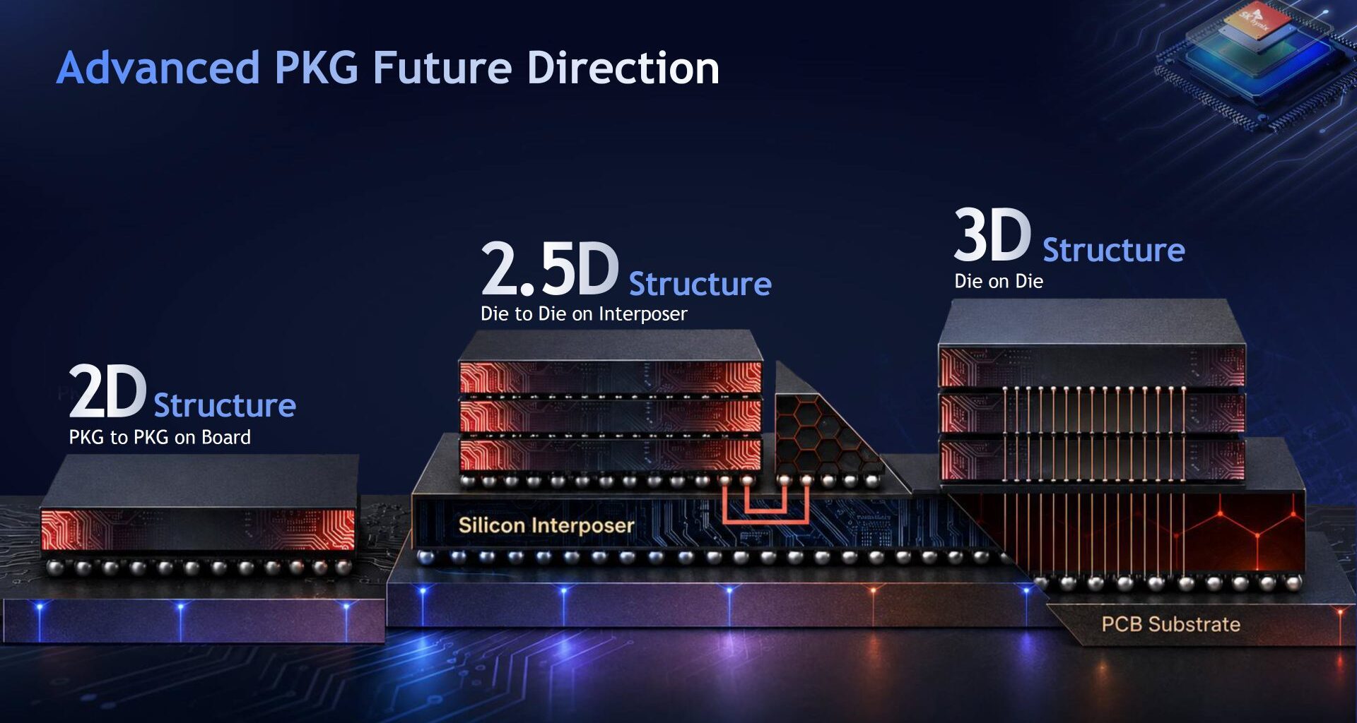
SK Hynix is leveraging advanced packaging technologies such as Intel’s EMIB for its next-gen HBM solutions, which will eventually enter the 3D packaging stage.
Scaling HBM Comes With Big Challenges & SK Hynix Is Leveraging Advanced Packaging Solutions To Address Them As It Ventures Into The 3D Era
At Hot Chips 2026, Jaesik Lee (VP Package Engineering at SK Hynix) presented the “Advanced Packaging for High-Bandwidth Memory” brief, which talks about how the company plans to leverage advanced packaging tech to accelerate its HBM roadmap.
The company started by presenting how HBM is currently built. The HBM structure consists of a 3D stacked structure that connects multiple core dies (DRAM ICs) to a base die using TSVs. HBM can currently reach a maximum height of 16 slices, or a 16-Hi stack.
There are four slices per rank, & a 16-Hi stack includes 4-ranks. There are four channels per slice, and these incorporate a total of 16 banks. The HBM and GPU are separate chips but are mounted on the same silicon interposer using 2.5D packaging. Each HBM module also contains 1024 IOs with 16-channels through the Si interposer. These connect the HBM stack to the XPU through a PHY.
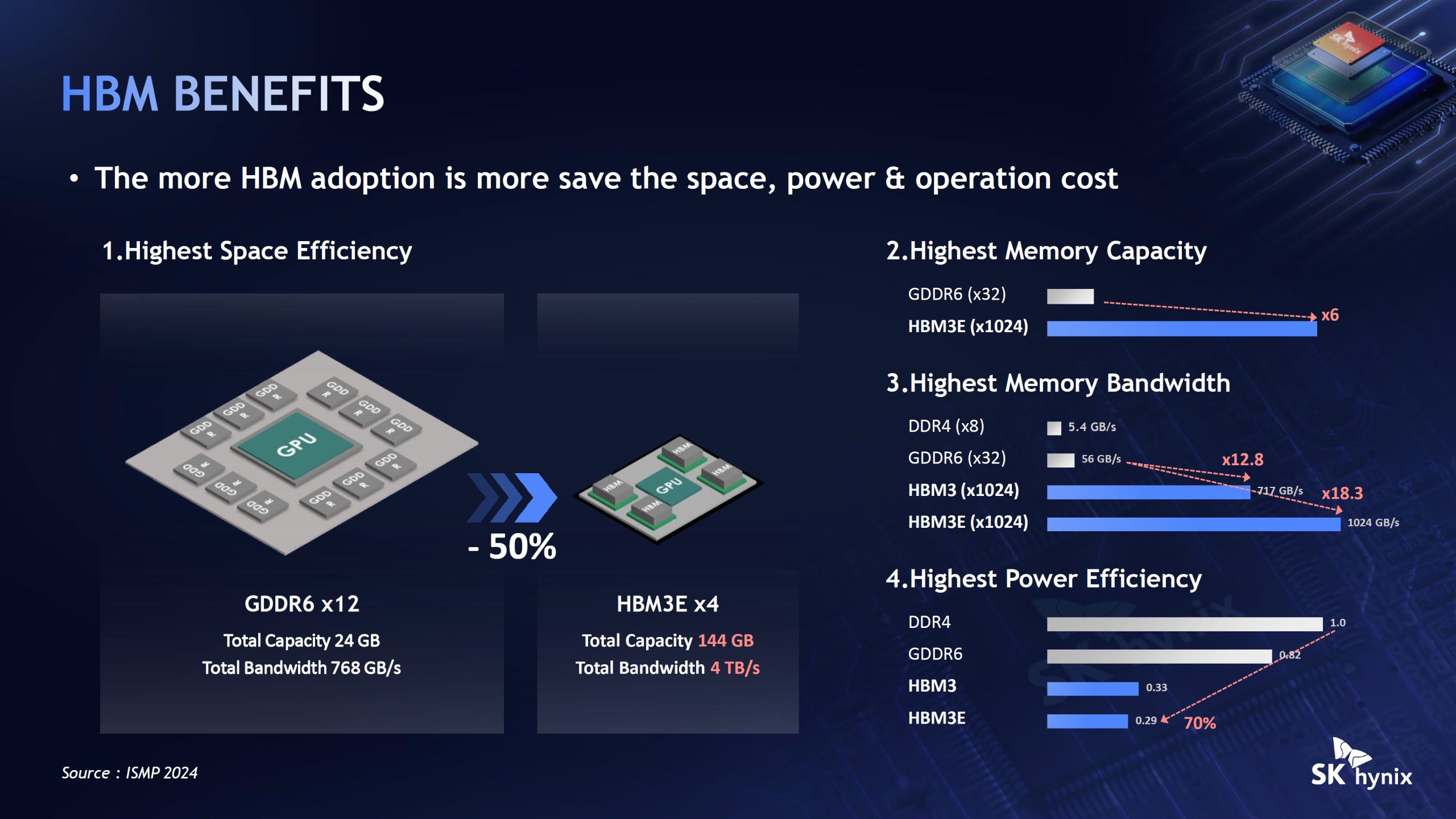
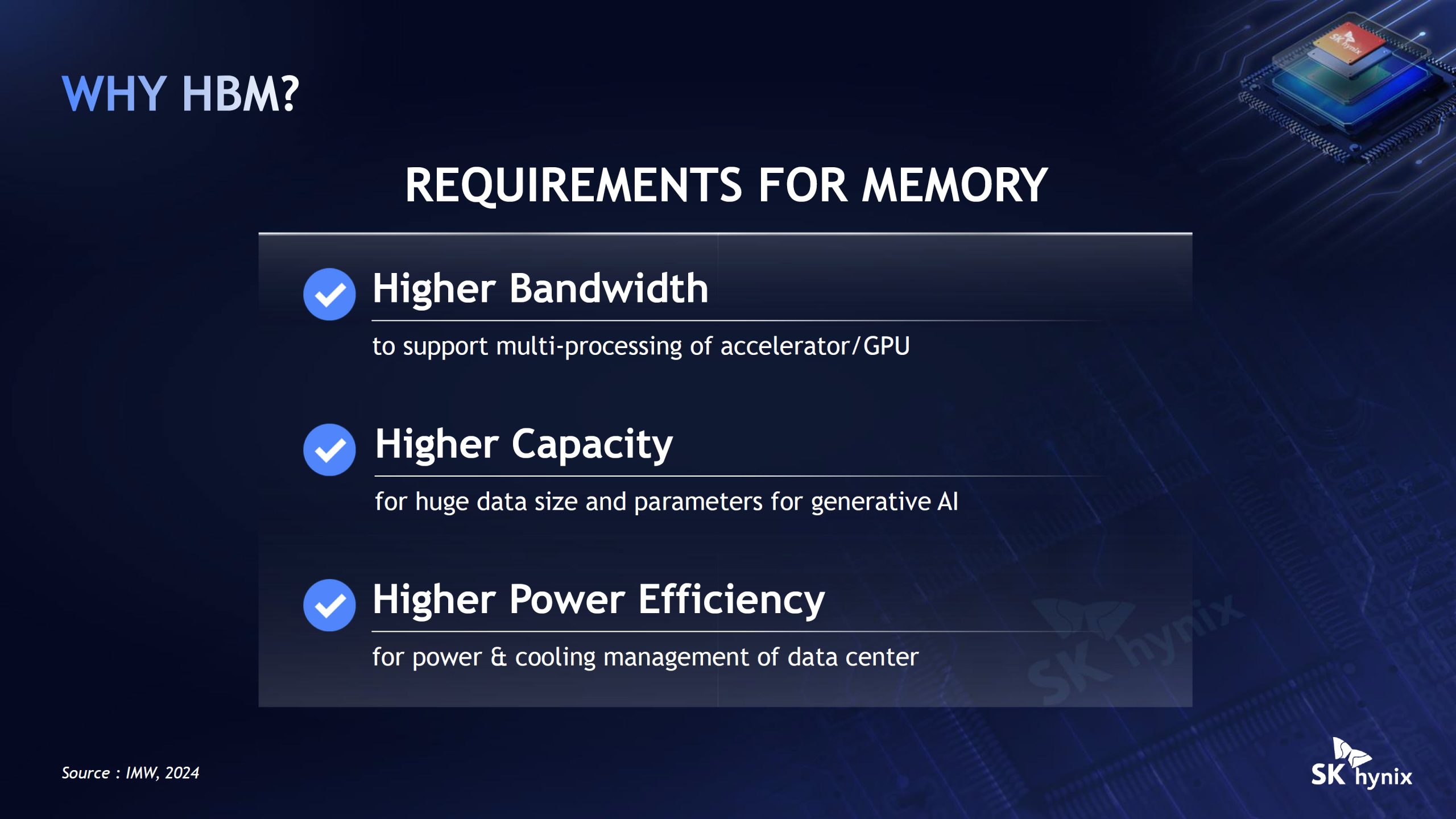
HBM is important as a DRAM solution because it saves space, power, and operating cost. A typical GDDR6 solution will carry 24 GB and 768 GB/s bandwidth, while an HBM3E solution with four stacks saves up to half the space while offering up to 144 GB capacity and 4 TB/s bandwidth.
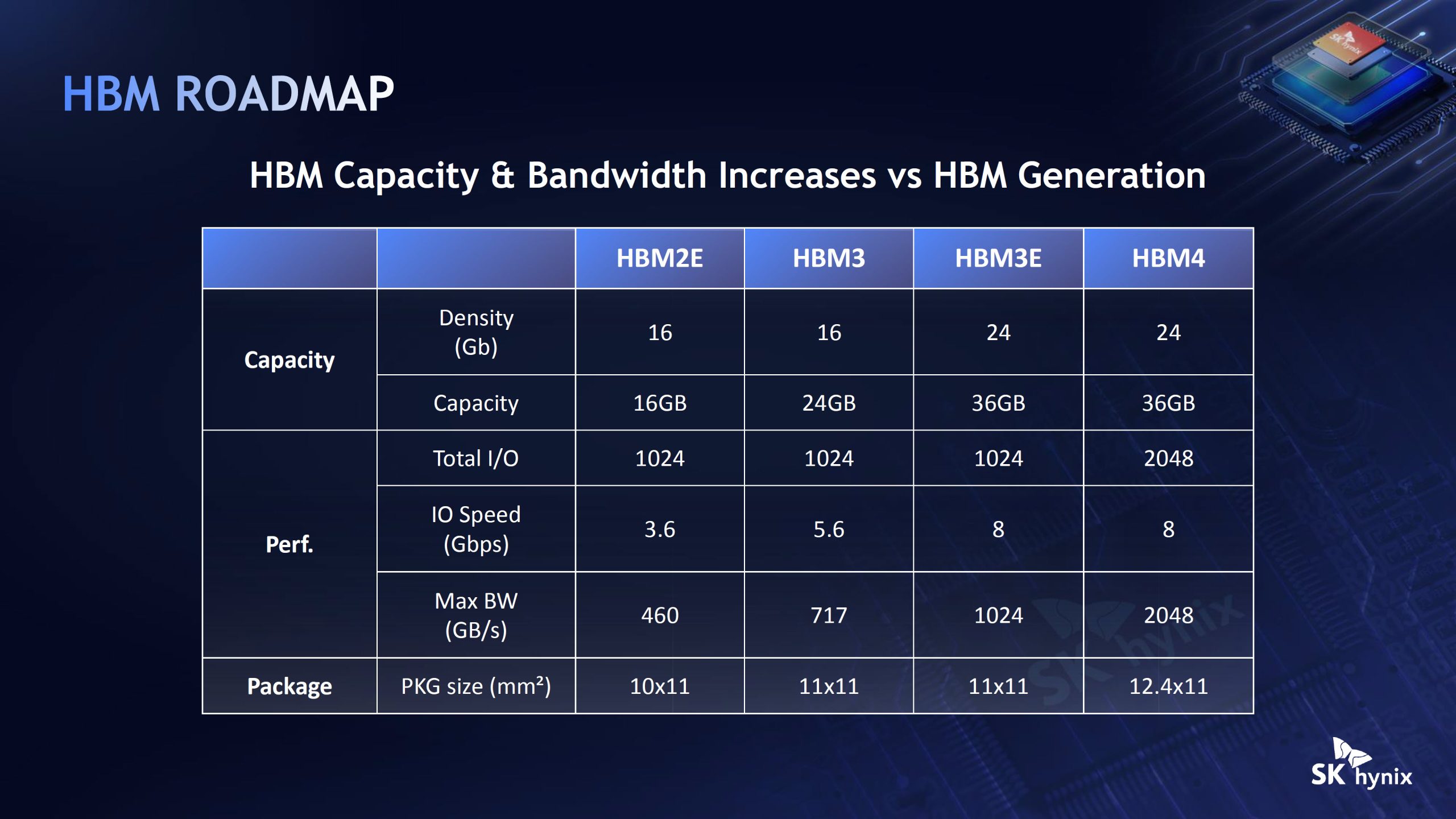
SK Hynix’s current roadmap includes HBM4 as the top-of-the-line product with up to 24 Gb DRAM densities, leading up to 36 GB capacities, a total of 2048 IO bits, up to 8 Gbps IO speeds, and 2048 GB/s bandwidth.
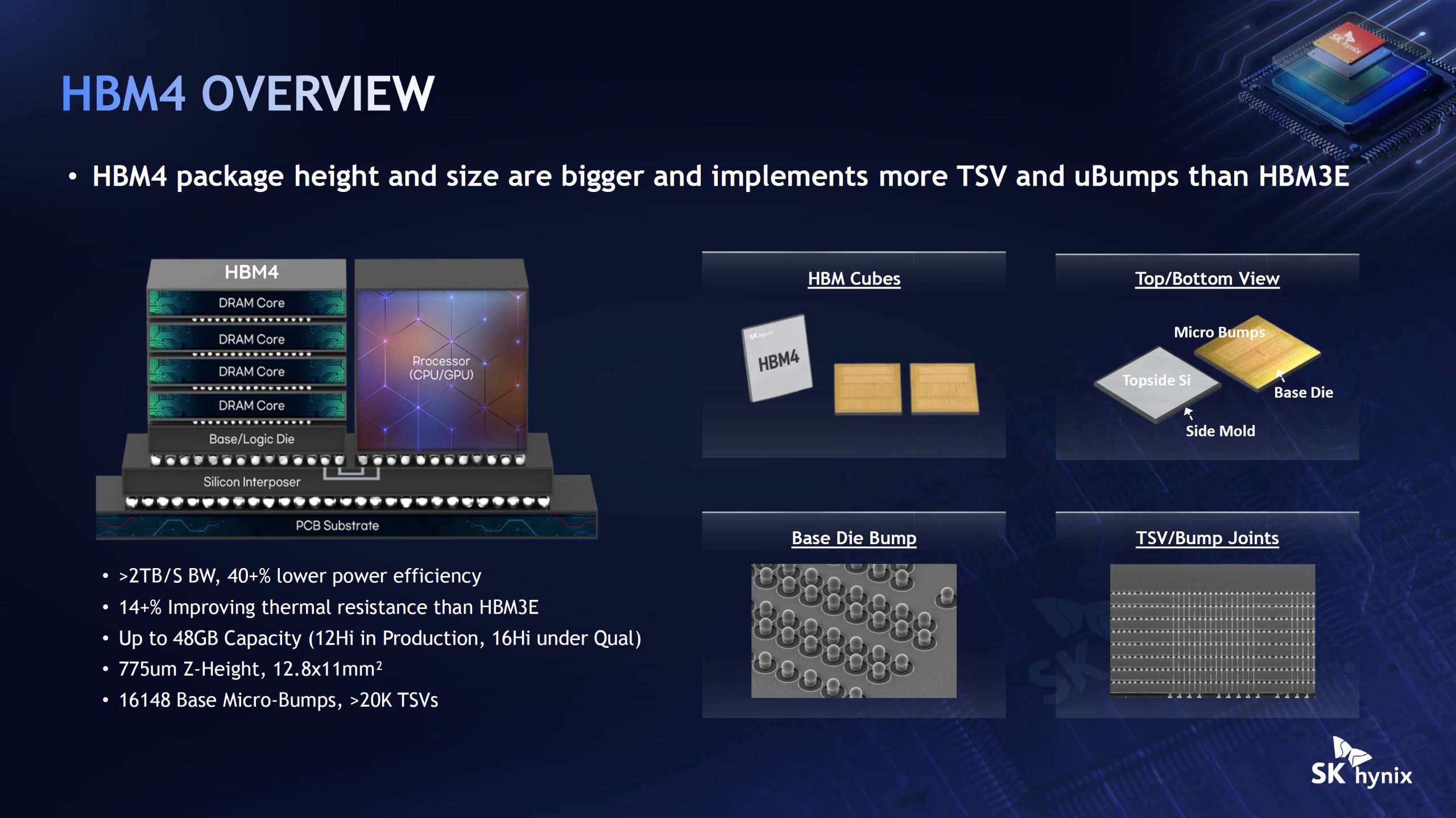
HBM4 comes with increased package height and size. It also integrates more TSVs & micro bumps than HBM3E. The result is:
>2 TB/s bandwidth
40+% Lower Power Efficiency
14+% improvement in thermal resistance than HBM3E
Up to 48 GB capacity (12-Hi in production, 16-Hi under qualification)
775um Z-Height, 12.8x11mm2
16,148 Base Micro-Bumps
>20K TSVs
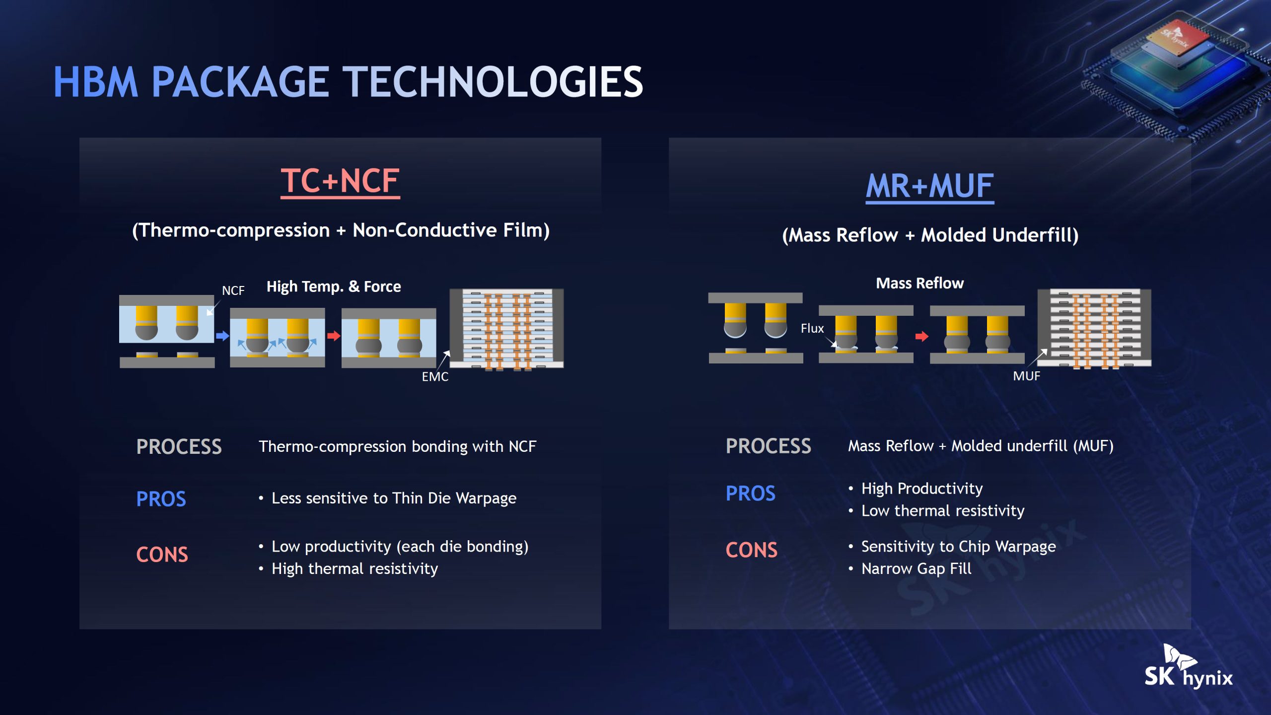
Currently, there are two main HBM packaging technologies: Thermo-Compression + Non-Conductive Film (TC+NCF), and Mass Reflow + Molded Underfill (MR+MUF). TC+NCF allows better resistance to die warpage issues but has higher thermal resistivity and lower productivity. MR+MUF offers higher productivity and low thermal resistivity but is more susceptible to chip warpage and also has gap fill drawbacks.
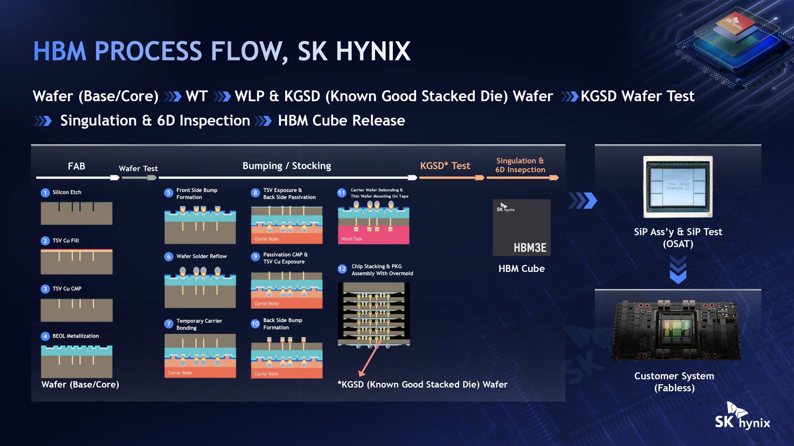
SK Hynix also highlights its HBM Process Flow, which includes six key stages from Fab to customer systems:
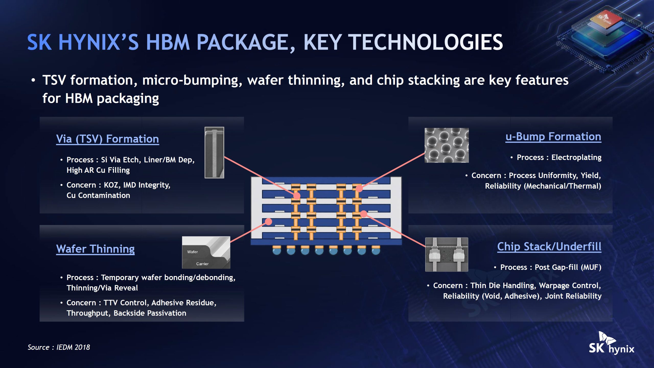
There are four key technologies that SK Hynix integrates within its HBM package; these include:
Via (TSV) Formation
Wafer Thining
u-Bump Formation
Chip Stack/Underfill
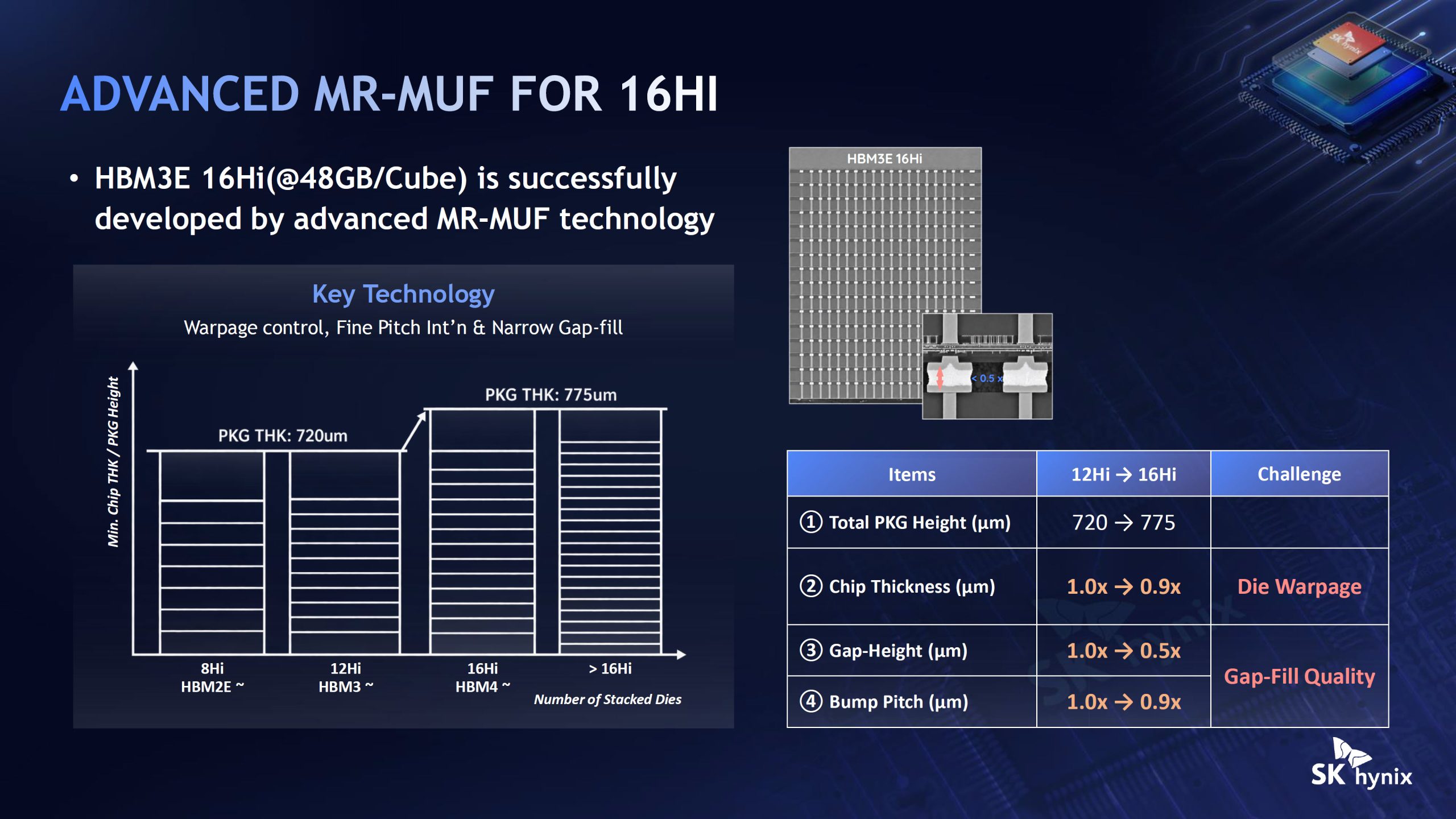
Advanced MR-MUF is already being leveraged by SK Hynix for its 16-Hi HBM3E solution with two new technologies: Warpage Control and Fine Pitch Int’n & Narrow Gap-fill. The total package height is increased to 775 microns while chip thickness is shrunk to 0.9x, gap height is reduced to 0.5x, and bump pitch is reduced to 0.9x.
However, moving forward, there are some key challenges that need to be addressed. First is the increase in HBM Power as bandwidth demand swells, and the second is the thermal issue along with the TSV Area. As the number of TSVs grows, the area continues to increase despite the TSV Pitch size shrinking. Furthermore, a near doubling of bandwidth every two generations puts a 2.2x thermal burden on existing processes and packaging technologies.
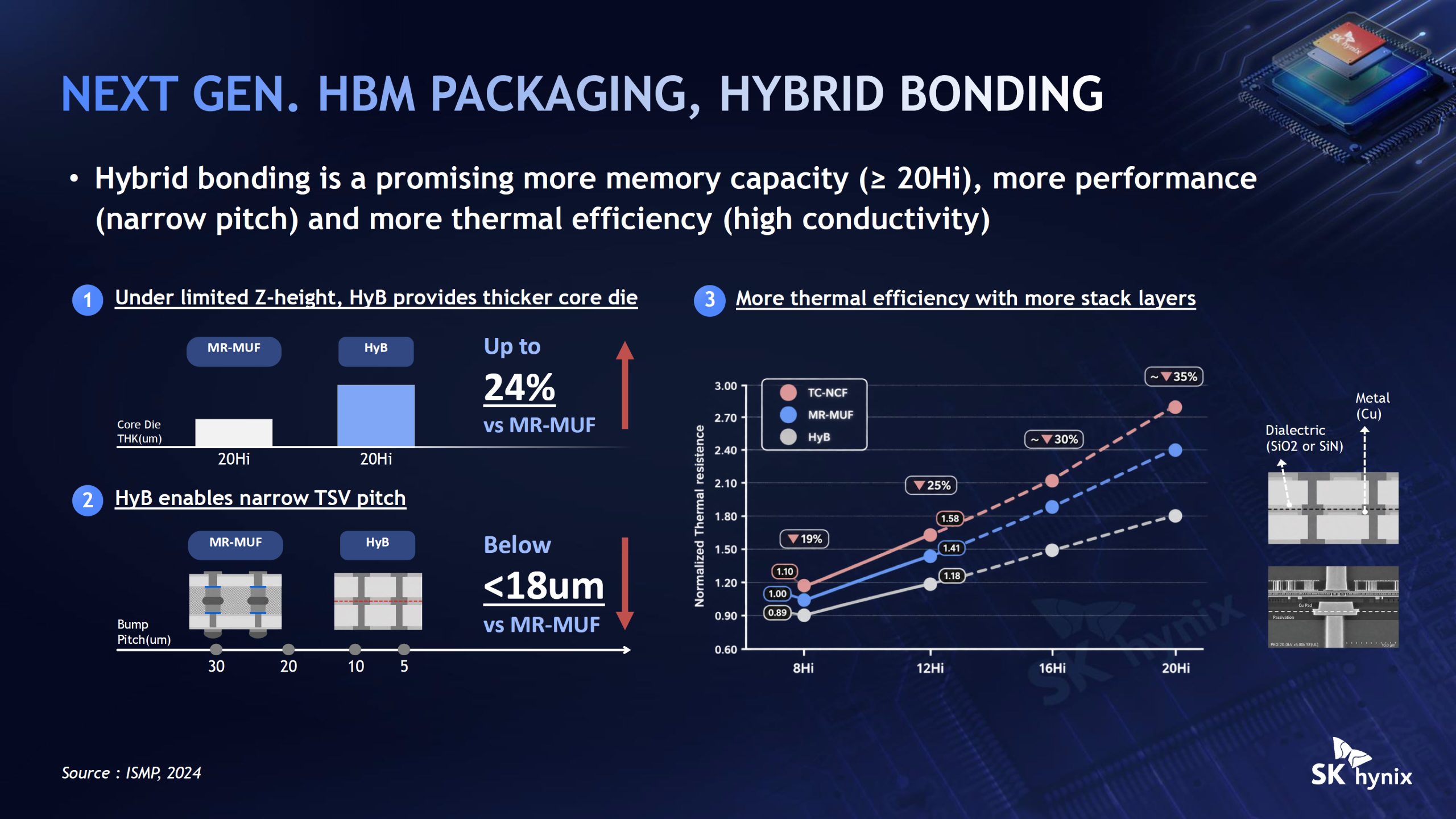
So SK Hynix is looking into future methodologies such as Hybrid Bonding to go beyond 16-Hi stacks, offering more performance through a narrower pitch, & offering better thermal efficiency through higher conductivity.
SK Hynix shows that Hybrid Bonding achieves a 24% thicker core die and a TSV pitch size of <18 microns versus MR-MUF processes. And even with an increased number of stack layers, Hybrid Bonding has 35% lower thermal resistance.
Like Samsung’s HPB (Heat Path Block), SK Hynix is working on its own localized hotspot mitigation tech called I-HBM, which embeds a high-thermal-conductivity and electrically insulating cooling component within the HBM D2D PHY area (near the hotspot), creating a dedicated heat path that offers an additional >30% reduction in thermal resistance.
Looking ahead, SK Hynix is looking to increase bandwidth through doubling of TSVs and higher IO speed with logic process integration, while power/PDN challenges will be addressed using the latest and optimized logic foundry processes with power TSVs spreading “everywhere” to greatly improve PDN.
The relentless push for higher power density, bandwidth, and stack heights in HBM technology brings significant thermal, mechanical, and packaging challenges, driven by thicker oxide layers, denser TSVs, and rising pin speeds.
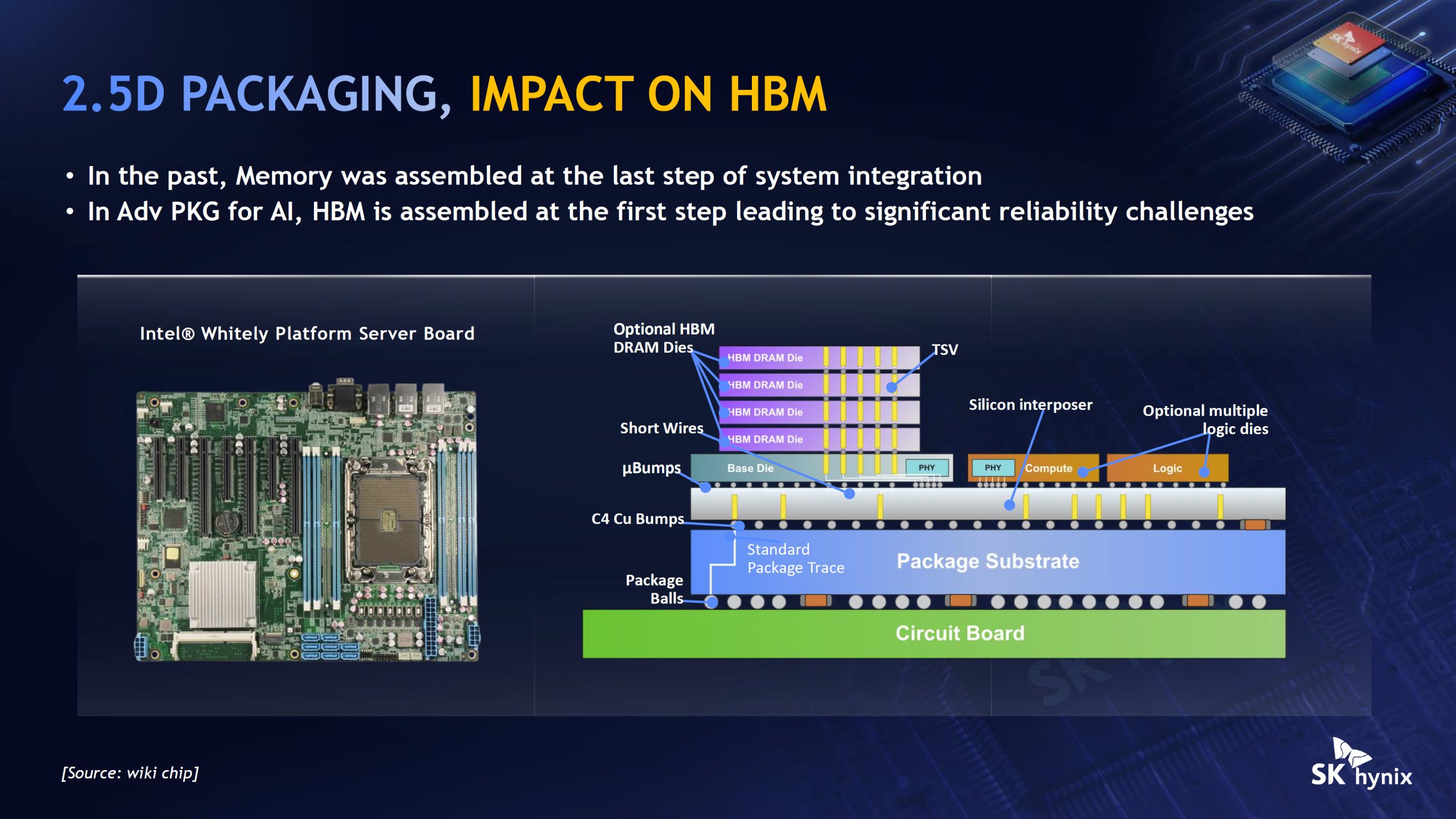
Innovations such as MLMO, optimized micro-bumps, emerging hybrid bonding (for improved thermal conductivity, process margins, and finer pitches), and hotspot solutions like IHBM are actively addressing these issues. Yet as stacks move toward 16–20 high and architectures evolve toward closer 3D integration with logic, success will demand even tighter co-optimization of design, materials, customer processes, and interposer technologies. Continued collaboration across the industry remains essential to meet future workload demands for both capacity and bandwidth.
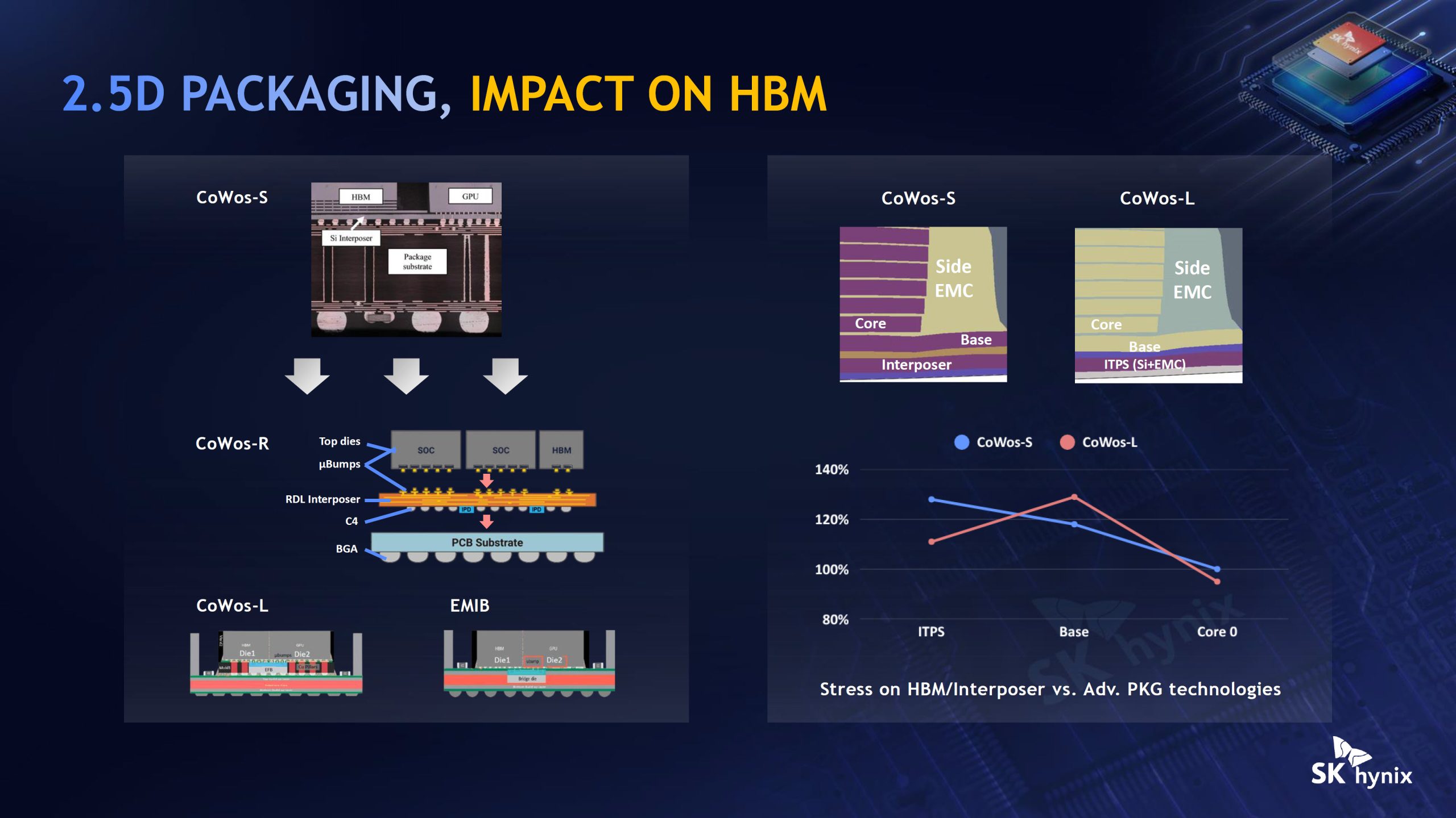
The company also teased Intel EMIB packaging technology in its 2.5D HBM solution slide alongside CoWoS-L, CoWoS-R, & CoWoS-S. Do note that Intel and SK Hynix are rumored to be involved in a JV on the memory front.
SK Hynix also showcased how different advanced packaging technologies stress on HBM/Interposer in different ways. And finally, SK Hynix is looking ahead with 3D integration in mind, which would allow them to stack HBM on top of accelerators, a move that everyone wants to make once advanced logic and advanced packaging technologies mature.

About the author: A Software Engineer by training and a PC enthusiast by passion, Hassan Mujtaba serves as Wccftech’s Senior Editor for hardware section. With years of experience in the industry, he specializes in deep-dive technical analysis of next-generation CPU and GPU architectures, motherboards, and cooling solutions. His work involves not only breaking news on upcoming technologies but also extensive hands-on reviews and benchmarking.
Follow Wccftech on Google to get more of our news coverage in your feeds.