
Design of the fully integrated flexible in-sensor computing circuit
Figure 1 illustrates the design of an in-sensor computing system based on fPCB-fabricated, non-aqueous gel-gated OECTs. The fully integrated system combines a wireless readout circuit with an OECT array for simultaneous biosensing and biocomputing (Fig. 1b–d). As shown in Fig. 1e, built on an fPCB, the system incorporates power management modules, analog front-end modules, and a built-in Bluetooth-Low-Energy (BLE) microcontroller for real-time signal acquisition and transmission.
Fig. 1: The design, architecture, and working principles of the fully integrated flexible in-sensor computing circuit based on non-aqueous gel-gated OECTs.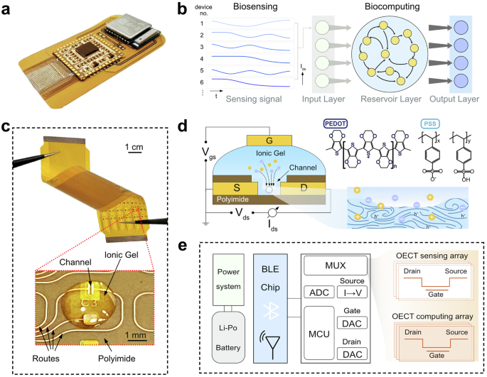
a Real image of the fPCB-fabricated fully integrated flexible in-sensor computing system. b The mechanism of the OECT-based biosensing and biocomputing. c Real images of the fPCB- fabricated electrodes. d The schematic of an OECT device. e Logic diagram of fully integrated flexible in-sensor computing circuits.
Fabrication of OECT arrays on fPCB
Figure 1c illustrates the resultant electrode arrays of 36 OECT units and the schematic of the single OECT device. A total of 108 interconnects were integrated within an area of 5 cm * 8 cm on the same layer. The feature size is about 100 µm, with channel width/length down to 100/100 µm. The fabrication of the electrodes of flexible OECTs starts with the photolithographic patterning of copper electrodes on the polyimide (PI) substrate, followed by the electroplating of a thin layer of gold (20 nm) to protect the copper (Fig. S1). The electrodes were further encapsulated by a second layer of PI (detailed in the experimental part).
Despite being protected with the gold layer (20 nm), Cu electrodes remain suffer from a redox instability with the electrolyte. This indicates the aqueous electrolyte can leak to the Cu layers to react. The reaction became noticeable at increased positive scanning voltages (> 0 V), limiting the use of fPCB-fabricated electrodes in water and aqueous hydrogel33. Nevertheless, we found the use of gel-based electrolytes (Fig. 2a) can efficiently mitigate the redox reaction of the Cu electrodes. As shown in Fig. 2b and Fig. S2, a negligible redox current was observed when the voltage was scanned between -1 V and +1 V, a typical voltage-operation window of OECTs. The results indicate the gel electrolytes can efficiently curb the diffusion of ions to the underlying Cu electrodes, thus maintaining the high stability of the electrodes under cyclic voltammetry (CV) scanning.
Fig. 2: Material design of OECTs fabricated with fPCB technology and ink-jet printing.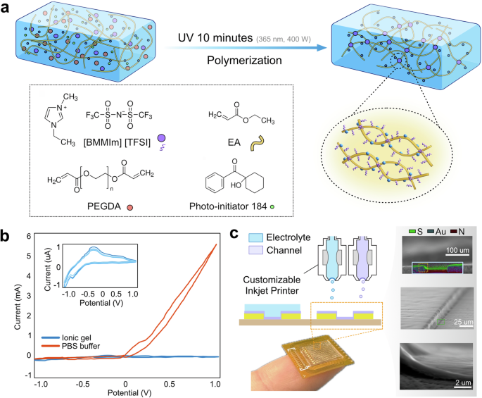
a Schematic and chemical structure of relevant chemicals to synthesize non-aqueous poly(ethyl acrylate) (PEA) ionic gel. b The comparison of CV curves of fPCB-fabricated electrodes (Au (200 nm)/Cu (30 µm)) with ionic gel and PBS as electrolytes, respectively. Inset: Zoom-in view of the CV response for the ionic gel. Three consecutive scans were performed to assess repeatability; the color intensity from dark to light blue represents the first to third scan, respectively. c Schematics of the customized inkjet printing platform for patterning of the channel and electrolyte. The scanning electron microscope (SEM) image shows the side-view of the interfaces between PEDOT:PSS channel and the electrodes.
The high stability of the fPCB-fabricated flexible electrode arrays in gel-electrolytes permits their use in developing all-solid-state devices and circuits. A typical application is to develop neuromorphic transistors to mimic the synaptic behaviors of neuron circuits25. For such applications, gel electrolytes are widely used and patterned between the gate and channel of OECTs to serve as ion reservoirs to regulate the device behaviors34,35.
The all-solid-state OECTs were fabricated by first fabricating the electrodes with the fPCB process, followed by the patterning of PEDOT:PSS channel and the gel electrolyte with a customizable inkjet printer (Fig. 2c), detailed in the experimental part). Crosslinkers were added to both the conducting polymer channel and the gel-electrolyte to improve their adhesion to the flexible substrates to prevent delamination over time and under bending conditions26. Because the feature size of the electrolyte is around 100 µm, alignment can be quickly completed between different functional layers.
OECTs characterizations
The overall performance of the resultant flexible all-solid-state OECTs is summarized in Fig. 3. Four types of typical curves were measured: output, transfer, transient, and cyclic stability. PEA was used as a solid-state electrolyte to prevent the reaction with copper electrodes. Gold-modified copper (area of 0.8 m2, thickness, 35 µm) was used as gate electrodes. The devices showed typical transistor characteristics, working in depletion mode (Fig. 3a, b). A high on/off ratio of ~1000 was extracted from the transfer curves (Vgs from -0.2 V to 0.8 V, source-drain voltage (Vds) from −0.1 to −0.6 V). Mobility of 1.1 cm2 V−1 s−1 is calculated according to the Bernards-Malliaras model10 (Fig. S3), indicating the high quality of the fPCB-printed electrodes and the inkjet-printed channels. The transfer curves showed minor hysteresis (Fig. S4) and good repeatability under cyclic scanning of Vgs between −0.1 and 0.8 V, which is within the safe electrochemical window for cooper (Fig. 3c). Besides, the transient response remains unchanged after 60 cycles of gate pulses, demonstrating the high stability of the devices thanks to the use of hydrogel electrolyte to prevent the oxidation of copper and the excellent adhesion between function layers because of the use of crosslinkers (Fig. 3d). The transient response also indicated a relatively fast dedoping/dedoping process of the channel due to the small geometrical size of the devices.
Fig. 3: Electrical characterizations of OECTs fabricated with fPCB technology and ink-jet printing.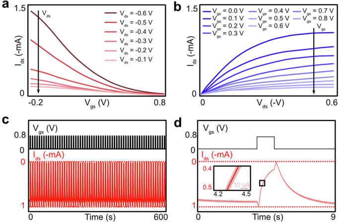
a The transfer curves (Vgs scanned from −0.2 to 0.8 V) at different Vds values (from -0.1 V to 0.6 V). b Output curves (Vgs scanned from 0 V to 0.8 V, Vds scanned from 0 V to -0.6 V). c Transient curves: a group of 60 pulses with 1.25 s width and 800 mV amplitude were applied at the gate electrode. d The red solid line shows the average Ids response of the 60 pulses in c) and the red shadow shows the current variation range during the transient characterization (< 10%), indicating the robustness of the device during cyclic measurements.
Homogeneity and flexibility of the fPCB-fabricated OECT arrays
To gain insight into the homogeneity and flexibility of our printed PEDOT:PSS films and the assembled solid-state OECTs on fPCB, we measured the channel current (Ids) and transconductance (gm) of an array consisting of 200 devices (Fig. 4a). The statical results show that the device yield is close to 100%, without notable failure operation, indicating good device homogeneity was achieved, benchmarkable to those patterned with state-of-the-art perylene or orthogonal photoresists36. To evaluate the flexibility of the devices, bending tests were performed by laminating the devices on 3D-printed testbeds with gradually changed bending curvatures (Fig. 4b). The transfer curves of the devices showed negligible change upon increasing bending curvature, the same for the extracted gm values, indicating the excellent conformability of the devices thanks to the thin thickness of the fPCB (thickness of 200 µm) and the improved softness of the PEDOT:PSS because the addition of stretchability enhancers (Fig. 4c, d)37.
Fig. 4: Homogeneity and flexibility characterizations of the flexible OECTs.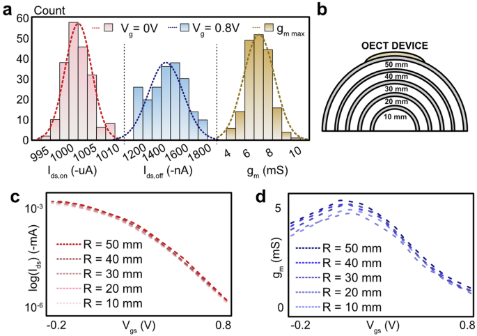
a Comparison of channel currents at Vgs = 0 V, Vgs = 0.8 V and maximum gm of 200 devices fabricated with fPCB technology. b Experimental setup of the flexibility test of OECTs. c, d Transfer and gm curves under different bending radius (from 10 to 50 mm).
Tactile sensing evaluation of fPCB-fabricated flexible OECTs
It can be easily imagined that the proposed fPCB-based fast, low-cost, and scalable fabrication methods for flexible OECTs have wide applications (Fig. S5)38. To demonstrate, we first evaluated the biosensing capabilities of these flexible OECT arrays. Here, we propose a rapid customizing OECT-based tactile sensor by integrating a micropyramid-structured ionic gel gated electrode of the fPCB-fabricated flexible OECTs, making it suitable for future personalized precision medicine and human–machine interaction (Fig. 5). The sensing mechanism of the fPCB-based OECT tactile sensor is illustrated in Fig. 5a and detailed in our previously reported work39. As shown in Fig. 5b, the fPCB-based OECT biosensor demonstrated highly sensitive responses to a wide range of applied pressures, ranging from 0.1 to 10 Pa. Figure 5c shows the hand-written experiment characters from “0” to “9” tested using the fPCB-based OECT tactile sensor array. Following binary processing and reshaping, the outcomes of the handwriting test with the tactile sensing array serve as the input dataset for the subsequent in-sensor computing process. The promising result from fPCB-based OECT tensile biosensors highlights its potential for real-time, reliable biosignals monitoring in precision wearable healthcare and human-machine interaction applications.
Fig. 5: Evaluation of flexible OECTs-based in-sensor computing.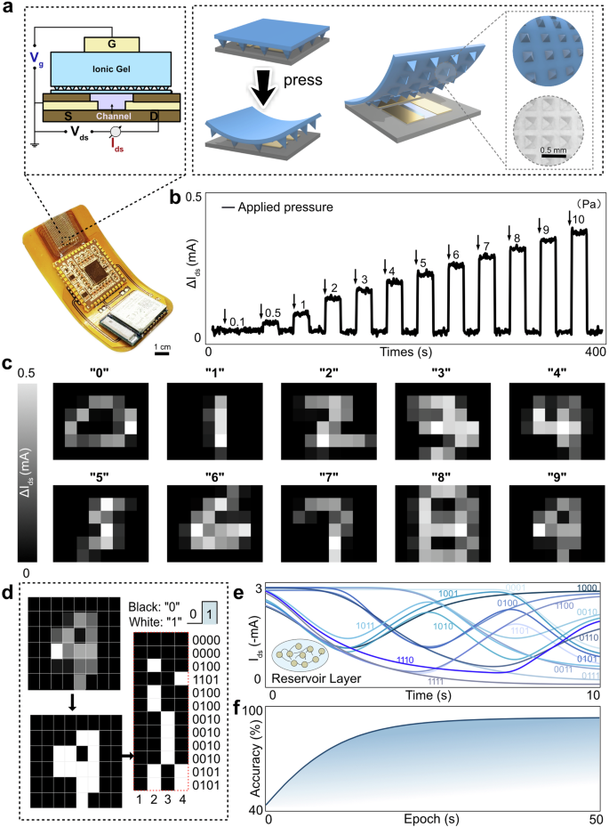
a shows the schematics of the fPCB-based OECT pressure sensor, also illustrating the sensing mechanism involving a pyramidal ionic gel electrolyte and a real image of the sensor array. b shows the variation in sensor current response to discrete pressure gradients. c Array of images showing the hand-written characters from “0” to “9” tested using the fPCB-based OECT pressure sensor array. d Decoding of the ten digital numbers for RC validation. The grayscale intensity in each image corresponds to the maximum current value detected during a 5-second sensing window. These data serve as a test dataset for reservoir computing applications. e The Ids progression curves corresponding to different Vgs patterns from 0000 to 1111. f Evolution of classification accuracy within 50 training epochs.
Neuromorphic function evaluation of fPCB-fabricated flexible OECTs
The high stability of the fPCB-fabricated flexible electrode arrays in gel electrolytes permits their use in all-solid-state devices. Another typical application of the device is to develop neuromorphic circuits to mimic the synaptic behaviors25,40,41. As shown in Fig. 5d, e, we further demonstrate the potential applications of those flexible OECT arrays with a specific neuromorphic computing framework, reservoir computing (RC)6,42,43,44. The Modified National Institute of Standards and Technology (MNIST) database was used as the training task with 12 flexible OECTs forming the reservoir layer and the siganl from the integarated tensile sensor array was used as the test task to further prove the in-sensing computing capibility of the fully-integrated flexible OECT in-sensor computing circuit. As shown in Fig. 5d, the inputdata of RC network was firstly encoded to different binary gate input patterns, where ‘1’ denotes applying a gate voltage (0.4 V) and ‘0’ denotes no voltage is applied (0 V). Then the OECTs-based reservoir layer outputs 16 distinguishable Ids values due to their excellent non-linear transient response (Fig. 5e. A pre-trained single connected layer serves as the output, with performance evaluated by confusion analysis (Fig. S6). The results show a > 90% accuracy of flexible OECT-based RC (Fig. 5f), permitting their deployment for practical applications such as wearable sensing and computing at the edge.
In conclusion, we presented a facile and scalable fabrication method that allows large-scale production of flexible all-solid-state OECTs. The electrode arrays and the encapsulation layers were fabricated using mature fPCB technology. The PEDOT:PSS channel and solid-state electrolyte were subsequently patterned on the fPCB with customizable inkjet printing methods. A small feature size of 100 µm was obtained for both the electrodes and the channel. Solid-state gels were found that can avoid the instability of the copper electrodes of the fPCB. Statistical characterizations demonstrated a high device yield (~100%), high homogeneity, and high flexibility were obtained simultaneously. The fast turnaround time, low cost, and scalability of the proposed fabrication methods pave the way for developing flexible solid-sate OECTs (and devices of similar kinds) for practical bioelectronic applications.